

Это старая версия документа!

Разработчик: PICMG https://www.picmg.org/
Страничка стандарта: https://www.picmg.org/openstandards/com-express/
Документация:
| Папка | link | |
| PICMG® COM.0 Revision 3 COM Express® Module Base Specification | PICMG | link |
| COM Express® Carrier Design Guide | PICMG | link |
| Design Guide for COM Express Type 6,7 & Type 10 Carrier Board | AAEON | link |
| COM EXPRESS CARRIER BOARD DESIGN GUIDE | iBASE | link |
| Type | Connectors | PCIe lanes | PEG | PCI | SATA | PATA IDE | LAN | Video | Serial | USB | Note | |
|---|---|---|---|---|---|---|---|---|---|---|---|---|
| 1 | AB only | 6 | No | No | 4 | Yes | 1 GbE | LVDS, VGA | Legacy | |||
| 2 | AB & CD | 22 | Yes | Yes | 4 | Yes | 1 GbE | PEG/SDVO,LVDS, VGA | Legacy | * | ||
| 3 | AB & CD | 22 | Yes | Yes | 4 | Yes | 3 GbE | PEG/SDVO, LVDS, VGA | Legacy | |||
| 4 | AB & CD | 32 | Yes | No | 4 | Yes | 1 GbE | PEG/SDVO, LVDS, VGA | Legacy | |||
| 5 | AB & CD | 32 | Yes | No | 4 | Yes | 3 GbE | PEG/SDVO, LVDS, VGA | Legacy | |||
| 6 | AB & CD | 24 | Yes | No | 4 | No | 1 GbE | 3 x DDI, VGA LVDS/eDP / Option for USB 4 | 2x RX/TX, GP_SPI, CAN | 4x USB 3.2/2.0 4x USB 2.0 | * | |
| 7 | AB & CD | 32 | Yes | Yes | 2 | No | 4x 10G (CEI side-band) 1 GbE | None | 2x RX/TX or CAN | 4x USB 3.2/2.0 4x USB 2.0 | * | |
| 10 | AB only | 4 | No | No | 2 | No | 1 GbE | 1x DDI, LVDS | 2x RX/TX, GP_SPI, CAN | 4x USB 3.2/2.0 | * |
| img | struct | ↓ link | pn | formfactor | manufacturer | cpu | emmc | ram | temprange | dp | hdmi | lvds | ethernet | dsi | csi | usb2 | usb3 | pcie | can | spi | i2c | smbus | uart | dimension | bios | datasheet_wiki | page_wiki |
|---|---|---|---|---|---|---|---|---|---|---|---|---|---|---|---|---|---|---|---|---|---|---|---|---|---|---|---|
 |  | adlink_nanox-el | nanoX-EL | COM Express Type 10 | Adlink | Intel Atom x6000E | 16/32/64 GB | 2/4/8/16 GB LPDDR4 | 0...+60 °C, -40...+85 °C | 1 DP/HDMI/VDI | Single Channel via eDP<>LVDS IC (or eDP) | 1 (2.5 GBit, SGMII) (GPY211/GPY215) | - | - | 6(8) | 2 | x4 x 1, x2 x 2, x1 x 4 gen 3 | 1 (in place of UART1) | + (BIOS, TPM) | 1 (from EC, option from CPU) | 1 | 2 (UART1 or CAN) (from EC, from CPU option) | 84 x 55 mm | AMI UEFI | link | page | |
 |  | advantech_som-7532 | SOM-7532 | COM Express Type 10 | Advantech | Intel Atom x6000E | 32/64 GB | 2/4/8/16 GB LPDDR4 | 0...+60 °C, -40...+85 °C | 1 DP/HDMI/VDI | Single Channel via eDP<>LVDS IC (or eDP) | 1 (2.5 GBit, SGMII) (I225) | - | - | 6(8) | 2 | x4 x 1, x2 x 2, x1 x 4 gen 3 | -? | + (BIOS, TPM 2.0) | 1 (from EC\CPU) | 1 (from EC\CPU) | 2 from EC/2 CAN friom EC/2 CAN from SoC | 84 x 55 mm | AMI UEFI 256Mbit | link | page | |
 | | congatec_conga-ma7 | Conga-MA7 | COM Express Type 10 | Congatec | Intel Atom x6000E | 32/64 GB | 2/4/8/16 GB LPDDR4 | 0...+60 °C, -40...+85 °C | 1 DP/HDMI/VDI | Single Channel via eDP<>LVDS IC (or eDP) | 1 (1 GBit, SGMII) (TI DP83867CS) | - | - | 6(8) | 2 | x4 x 1, x2 x 2, x1 x 4 gen 3 | -? | + (BIOS, TPM 2.0) | 1 (from EC\CPU) | 1 (from EC\CPU) | 2 from EC/2 CAN friom EC/2 CAN from SoC | 84 x 55 mm | AMI UEFI 256Mbit | link | page | |
 | | kontron_come-mel10 | COMe-mEL10 | COM Express Type 10 | Kontron | Intel Atom x6000E | 16/32 GB | 2/4/8 GB LPDDR4 | 0...+60 °C, -40...+85 °C | 1 DP/HDMI/VDI | Single Channel via eDP<>LVDS IC (or eDP) | 1 (2.5 GBit, SGMII) (GPY115/GPY215) | - | - | 6(8) (port7 client) | 2 | x4 x 1, x2 x 2, x1 x 4 gen 3 | 2 (in place of UART0/1) | + (BIOS, TPM) | 1 (from EC) | 1 | 2 (UART or CAN) (from EC, from CPU option) | 84 x 55 mm | AMI Aptio V uEFI | link | page | |
 |  | portwell_pcom-b634vg | PCOM-B634VG | COM Express Type 6 Basic | Portwell | Intel Pentium/Xeon D-1500 | - | up to 48 GB DDR4 (3 x SODIMM) | -40...+80 °C | 1 (SM750) | 1 (1 GBit) (I210-IT) | 8 | 3 | x16 gen 3 x 1, x1 gen 2 x 8 | 2 | link | page | ||||||||||
 |  | portwell_pcom-ba02gl | PCOM-BA02GL | COM Express Type 10 | Portwell | Intel Atom x6000E | 16/32 GB | 4/8/16 GB LPDDR4 | 0...+60 °C, -40...+85 °C | 1 DP/HDMI/VDI | Single Channel via eDP<>LVDS IC (or eDP) | 1 (1GBit? 2.5 GBit?, SGMII? PCIe?) (GPY215? I210AT?) | - | - | 6(8) | 2 | x4 x 1, x2 x 2, x1 x 4 gen 3 | -? | + (BIOS, TPM 2.0) | 1 (from EC\CPU) | 1 (from EC\CPU) | 2 from EC | 84 x 55 mm | AMI BIOS | link | page | |
 |  | tq-embedded_tqmxe40m | TQMxE40m | COM Express Type 10 | TQ-Embedded | Intel Atom® x6000 series Elkhart Lake | 8...256 GB | 4/8/16 GB LPDDR4/4x | 0...+60 °C, -40...+85 °C | 1 (or hdmi) | 1 (or dp) | 1 1ch (or edp) | 1 1G (Marvell 88E1512) | - | - | 6(8) | 2 | 4 gen 3 (1x4, 2x2, 4x1) | 1 (or SER1) | 1 | 1/2 optional | 1 | 2/1 + 1 CAN (2 full optional) | 82x50 | InsydeH2O 64bit uEFI | link | page |

Толщина платы, фаска:
Модуль
Модуль
KeepOut area:
Ответная часть на материнской плате:
| module | single | Tyco Electronics | 3-6318490-6 | link step | 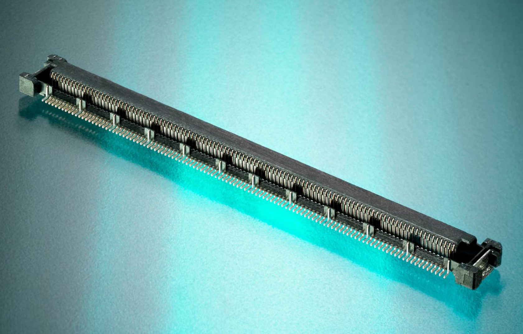 |
|
| module | single | Foxconn | QT012206-1031-2H | |||
| module | single | ept | 402-51101-51 | |||
| module | single | KLS | L-KLS1-B0705-545F220-T3R ???? | link | ||
| module | double | Tyco Electronics | 3-1827231-6 | link | ||
| module | double | Foxconn | QT012206-1041-3H | |||
| module | double | ept | 402-51501-51 | |||
| carrier | single | 5mm | Tyco Electronics | 3-1827253-6 | link | 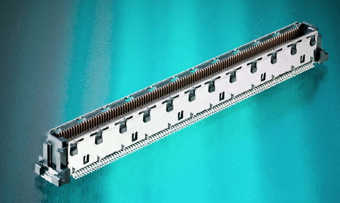 |
| carrier | single | 5mm | Foxconn | QT002206-2131-3H | ||
| carrier | single | 5mm | ept | 401-51101-51 | ||
| carrier | double | 5mm | Tyco Electronics | 3-1827233-6 | link | |
| carrier | double | 5mm | Foxconn | QT002206-2141-3H | ||
| carrier | double | 5mm | ept | 401-51501-51 | ||
| carrier | single | 8mm | Tyco Electronics | 3-6318491-6 | link | |
| carrier | single | 8mm | Foxconn | QT002206-4131-3H | ||
| carrier | single | 8mm | ept | 401-55101-51 | ||
| carrier | double | 8mm | Tyco Electronics | 3-5353652-6 | link | |
| carrier | double | 8mm | Foxconn | QT002206-4141-3H | ||
| carrier | double | 8mm | ept | 401-55501-51 | ||
| Pin # | Pin Des | Pin Name | Group | Pin Type | Pwr Rail Tolerance | Notes | Description |
|---|---|---|---|---|---|---|---|
| 196 | B98 | DDI0_CTRLCLK_AUX+ | DDI | I/O PCIE I/O OD CMOS | DP: AC coupled on Module HDMI: 3.3V / 3.3V | AC 100nF? | DP: DP AUX+ function if DDI[0]_DDC_AUX_SEL is no connect, Half-duplex bi-directional AUX channel for services such as link configuration or maintenance and EDID access HDMI: HDMI/DVI I2C CTRLCLK if DDI[0]_DDC_AUX_SEL is pulled high, HDMI/DVI I2C control clock |
| 198 | B99 | DDI0_CTRLDATA_AUX- | DDI | I/O PCIE I/O OD CMOS | DP: AC coupled on Module HDMI: 3.3V / 3.3V | AC 100nF? | DP: DP AUX- function if DDI[0]_DDC_AUX_SEL is no connect, Half-duplex bi-directional AUX channel for services such as link configuration or maintenance and EDID access HDMI: HDMI/DVI I2C CTRLDATA if DDI[0]_DDC_AUX_SEL is pulled high, HDMI/DVI I2C control data |
| 190 | B95 | DDI0_DDC_AUX_SEL | DDI | I CMOS | 3.3V / 3.3V | PD with 1M | Selects the function of DDI[0]_CTRLCLK_AUX+ and DDI[0]_CTRLDATA_AUX-. This pin shall have a 1M pull-down to logic ground on the Module. If this input is unconnected the AUX pair is used for the DP AUX+/- signals. If pulled-high the AUX pair contains the CRTLCLK and CTRLDATA signals. |
| 178 | B89 | DDI0_HPD | DDI | I CMOS | 3.3V / 3.3V | DDI Hot-Plug Detect DP: DP0_HPD Detection of Hot Plug / Unplug and notification of the link layer HDMI: HDMI0_HPD, HDMI/DVI Hot-Plug Detect |
|
| 144 | B72 | DDI0_PAIR0- | DDI | O PCIE | AC coupled off Module | DDI 0 Pair[0:3] differential pairs DP: DP0_LANE0-, Uni-directional main link for the transport of isochronous streams and secondary data packets HDMI: TMDS0_DATA2-, HDMI/DVI TMDS lanes 0, 1 and 2 differential pairs |
|
| 142 | B71 | DDI0_PAIR0+ | DDI | O PCIE | AC coupled off Module | DDI 0 Pair[0:3] differential pairs DP: DP0_LANE0+, Uni-directional main link for the transport of isochronous streams and secondary data packets HDMI: TMDS0_DATA2+, HDMI/DVI TMDS lanes 0, 1 and 2 differential pairs |
|
| 148 | B74 | DDI0_PAIR1- | DDI | O PCIE | AC coupled off Module | DDI 0 Pair[0:3] differential pairs DP: DP0_LANE1-, Uni-directional main link for the transport of isochronous streams and secondary data packets HDMI: TMDS0_DATA1-, HDMI/DVI TMDS lanes 0, 1 and 2 differential pairs |
|
| 146 | B73 | DDI0_PAIR1+ | DDI | O PCIE | AC coupled off Module | DDI 0 Pair[0:3] differential pairs DP: DP0_LANE1+, Uni-directional main link for the transport of isochronous streams and secondary data packets HDMI: TMDS0_DATA1+, HDMI/DVI TMDS lanes 0, 1 and 2 differential pairs |
|
| 152 | B76 | DDI0_PAIR2- | DDI | O PCIE | AC coupled off Module | DDI 0 Pair[0:3] differential pairs DP: DP0_LANE2-, Uni-directional main link for the transport of isochronous streams and secondary data packets HDMI: TMDS0_DATA0-, HDMI/DVI TMDS lanes 0, 1 and 2 differential pairs |
|
| 150 | B75 | DDI0_PAIR2+ | DDI | O PCIE | AC coupled off Module | DDI 0 Pair[0:3] differential pairs DP: DP0_LANE2-, Uni-directional main link for the transport of isochronous streams and secondary data packets HDMI: TMDS0_DATA0-, HDMI/DVI TMDS lanes 0, 1 and 2 differential pairs |
|
| 164 | B82 | DDI0_PAIR3- | DDI | O PCIE | AC coupled off Module | DDI 0 Pair[0:3] differential pairs DP: DP0_LANE3-, Uni-directional main link for the transport of isochronous streams and secondary data packets HDMI: TMDS0_CLK-, HDMI/DVI TMDS Clock differential pair |
|
| 162 | B81 | DDI0_PAIR3+ | DDI | O PCIE | AC coupled off Module | DDI 0 Pair[0:3] differential pairs DP: DP0_LANE3+, Uni-directional main link for the transport of isochronous streams and secondarydata packets HDMI: TMDS0_CLK+, HDMI/DVI TMDS Clock differential pair |
|
| 4 | B2 | GBE0_ACT# | GBE | OD CMOS | 3.3V Suspend/ 3 3V | Gigabit Ethernet Controller 0 activity indicator, active low. | |
| 27 | A14 | GBE0_CTREF | GBE | REF | GND min 3.3V max | Reference voltage for Carrier Board Ethernet channel 0 magnetics center tap. The reference voltage is determined by the requirements of the Module PHY and may be as low as 0V and as high as 3.3V. The reference voltage output shall be current limited on the Module. In the case in which the reference is shorted to ground, the current shall be limited to 250 mA or less. | |
| 15 | A8 | GBE0_LINK# | GBE | OD CMOS | 3.3V Suspend/ 3 3V | Gigabit Ethernet Controller 0 link indicator, active low. | |
| 7 | A4 | GBE0_LINK100# | GBE | OD CMOS | 3.3V Suspend/ 3 3V | Gigabit Ethernet Controller 0 100 Mbit / sec link indicator, active low | |
| 9 | A5 | GBE0_LINK1000# | GBE | OD CMOS | 3.3V Suspend/ 3 3V | Gigabit Ethernet Controller 0 1000 Mbit / sec link indicator, active low. | |
| 23 | A12 | GBE0_MDI0- | GBE | I/O Analog | 3.3V max Suspend | 100R??? | Gigabit Ethernet Controller 0: Media Dependent Interface Differential Pairs 0,1,2,3. The MDI can operate in 1000, 100 and 10 Mbit / sec modes. Some pairs are unused in some modes, per the following: 10,100Mbit — MDI0-TX, MDI1-RX |
| 25 | A13 | GBE0_MDI0+ | GBE | I/O Analog | 3.3V max Suspend | 100R??? | Gigabit Ethernet Controller 0: Media Dependent Interface Differential Pairs 0,1,2,3. The MDI can operate in 1000, 100 and 10 Mbit / sec modes. Some pairs are unused in some modes, per the following: 10,100Mbit — MDI0-TX, MDI1-RX |
| 17 | A9 | GBE0_MDI1- | GBE | I/O Analog | 3.3V max Suspend | 100R??? | Gigabit Ethernet Controller 0: Media Dependent Interface Differential Pairs 0,1,2,3. The MDI can operate in 1000, 100 and 10 Mbit / sec modes. Some pairs are unused in some modes, per the following: 10,100Mbit — MDI0-TX, MDI1-RX |
| 19 | A10 | GBE0_MDI1+ | GBE | I/O Analog | 3.3V max Suspend | 100R??? | Gigabit Ethernet Controller 0: Media Dependent Interface Differential Pairs 0,1,2,3. The MDI can operate in 1000, 100 and 10 Mbit / sec modes. Some pairs are unused in some modes, per the following: 10,100Mbit — MDI0-TX, MDI1-RX |
| 11 | A6 | GBE0_MDI2- | GBE | I/O Analog | 3.3V max Suspend | 100R??? | Gigabit Ethernet Controller 0: Media Dependent Interface Differential Pairs 0,1,2,3. The MDI can operate in 1000, 100 and 10 Mbit / sec modes. Some pairs are unused in some modes, per the following: 10,100Mbit — MDI0-TX, MDI1-RX |
| 13 | A7 | GBE0_MDI2+ | GBE | I/O Analog | 3.3V max Suspend | 100R??? | Gigabit Ethernet Controller 0: Media Dependent Interface Differential Pairs 0,1,2,3. The MDI can operate in 1000, 100 and 10 Mbit / sec modes. Some pairs are unused in some modes, per the following: 10,100Mbit — MDI0-TX, MDI1-RX |
| 3 | A2 | GBE0_MDI3- | GBE | I/O Analog | 3.3V max Suspend | 100R??? | Gigabit Ethernet Controller 0: Media Dependent Interface Differential Pairs 0,1,2,3. The MDI can operate in 1000, 100 and 10 Mbit / sec modes. Some pairs are unused in some modes, per the following: 10,100Mbit — MDI0-TX, MDI1-RX |
| 5 | A3 | GBE0_MDI3+ | GBE | I/O Analog | 3.3V max Suspend | 100R??? | Gigabit Ethernet Controller 0: Media Dependent Interface Differential Pairs 0,1,2,3. The MDI can operate in 1000, 100 and 10 Mbit / sec modes. Some pairs are unused in some modes, per the following: 10,100Mbit — MDI0-TX, MDI1-RX |
| 97 | A49 | GBE0_SDP | GBE | I/O | 3.3V Suspend/ 3 3V | Gigabit Ethernet Controller 0 Software-Definable Pin. Can also be used for IEEE1588 support such as a 1pps signal. See section 4.3.5 for details. | |
| 107 | A54 | GPI0 | GPIO SDIO | I CMOS IO CMOS | 3.3V / 3.3V | GPIO: GPI0, General purpose input pins. Pulled high internally on the Module. SDIO: SDIO_DAT[0], SDIO Data lines. These signals operate in push-pull mode. Maps to GPI[0:3]. |
|
| 125 | A63 | GPI1 | GPIO SDIO | I CMOS IO CMOS | 3.3V / 3.3V | GPIO: GPI1, General purpose input pins. Pulled high internally on the Module. SDIO: SDIO_DAT[1], SDIO Data lines. These signals operate in push-pull mode. Maps to GPI[0:3]. |
|
| 133 | A67 | GPI2 | GPIO SDIO | I CMOS IO CMOS | 3.3V / 3.3V | GPIO: GPI2, General purpose input pins. Pulled high internally on the Module. SDIO: SDIO_DAT[2], SDIO Data lines. These signals operate in push-pull mode. Maps to GPI[0:3]. |
|
| 169 | A85 | GPI3 | GPIO SDIO | I CMOS IO CMOS | 3.3V / 3.3V | GPIO: GPI3, General purpose input pins. Pulled high internally on the Module. SDIO: SDIO_DAT[3], SDIO Data lines. These signals operate in push-pull mode. Maps to GPI[0:3]. |
|
| 185 | A93 | GPO0 | GPIO SDIO | O CMOS | 3.3V / 3.3V | GPIO: GPO0, General purpose output pins. Upon a hardware reset, these outputs should be low. SDIO: SDIO_CLK, SDIO Clock. With each cycle of this signal a one-bit transfer on the command and each data line occurs. This signal has maximum frequency of 48 MHz. Maps to GPO0. |
|
| 108 | B54 | GPO1 | GPIO SDIO | O CMOS | 3.3V / 3.3V | GPIO: GPO1, General purpose output pins. Upon a hardware reset, these outputs should be low. SDIO: SDIO_CMD, SDIO Command/Response. This signal is used for card initialization and for command transfers. During initialization mode this signal is open drain. During command transfer this signal is in push-pull mode. Maps to GPO1. |
|
| 114 | B57 | GPO2 | GPIO SDIO | O CMOS I CMOS | 3.3V / 3.3V | GPIO: GPO2, General purpose output pins. Upon a hardware reset, these outputs should be low. SDIO: SDIO_WP, SDIO Write Protect. This signal denotes the state of the write-protect tab on SD cards. Maps to GPO2; used as an input when used for SD card support. |
|
| 126 | B63 | GPO3 | GPIO SDIO | O CMOS I CMOS | 3.3V / 3.3V | GPIO: GPO3, General purpose output pins. Upon a hardware reset, these outputs should be low. SDIO: SDIO_CD#, SDIO Card Detect. This signal indicates when a SDIO/MMC card is present. Maps to GPO3; used as an input when used for SD card support. |
|
| 63 | A32 | HDA_BITCLK | HDA | I/O CMOS | 3.3V/3.3V | Serial data clock generated by the external CODEC(s). | |
| 59 | A30 | HDA_RST# | HDA | O CMOS | 3.3V Suspend/ 3 3V | Reset output to CODEC, active low | |
| 60 | B30 | HDA_SDIN0 | HDA | I/O CMOS | 3.3V Suspend/ 3 3V | Serial TDM data inputs from up to 3 CODECs. | |
| 58 | B29 | HDA_SDIN1 | HDA | I/O CMOS | 3.3V Suspend/ 3 3V | Serial TDM data inputs from up to 3 CODECs. | |
| 56 | B28 | HDA_SDIN2 | HDA | I/O CMOS | 3.3V Suspend/ 3 3V | Serial TDM data inputs from up to 3 CODECs. | |
| 65 | A33 | HDA_SDOUT | HDA | O CMOS | 3.3V/3.3V | Serial TDM data output to the CODEC. | |
| 57 | A29 | HDA_SYNC | HDA | O CMOS | 3.3V/3.3V | Sample-synchronization signal to the CODEC(s) | |
| 66 | B33 | I2C_CK | I2C | I/O OD CMOS | 3.3V Suspend/ 3.3V | PU to 3.3V Standby with 2.2K | General purpose I2C port clock output |
| 68 | B34 | I2C_DAT | I2C | I/O OD CMOS | 3.3V Suspend/ 3.3V | PU to 3.3V Standby with 2.2K | General purpose I2C port data I/O line |
| 67 | A34 | BIOS_DIS0#/ESPI_SAFS | LPC_ESPI | I CMOS | NA | PU to 3.3V with 10K | Selection strap to determine the BIOS boot device. The Carrier should only float these or pull them low, please refer to Table 4.13 for strapping options of BIOS disable signals. |
| 176 | B88 | BIOS_DIS1# | LPC_ESPI | I CMOS | NA | PU to 3.3V with 10K | Selection strap to determine the BIOS boot device. The Carrier should only float these or pull them low, please refer to Table 4.13 for strapping options of BIOS disable signals. |
| 94 | B47 | ESPI_EN# | LPC_ESPI | I CMOS | NA | PU to logic high with 20K | This signal is used by he Carrier to indicate the operating mode of the LPC/eSPI bus. If left unconnected on he carrier, LPC mode (default) is selected. If pulled to GND on the carrier, eSPI mode is selected. This signal is pulled to a logic high on the module through a resistor. The Carrier should only float his line or pull it low. |
| 8 | B4 | LPC_AD0/ESPI_IO_0 | LPC_ESPI | I/O CMOS | LPC:3.3V / 3.3V ESPI:1.8V Suspend / 1.8V | ser 22R ??? | LPC: LPC multiplexed address, command and data bus ESPI: eSPI Master Data Input / Outputs These are bi-directional input/output pins used to transfer data between master and slaves. Multiplexed with LPC_AD[0:3] |
| 10 | B5 | LPC_AD1/ESPI_IO_1 | LPC_ESPI | I/O CMOS | LPC:3.3V / 3.3V ESPI:1.8V Suspend / 1.8V | ser 22R ??? | LPC: LPC multiplexed address, command and data bus ESPI: eSPI Master Data Input / Outputs These are bi-directional input/output pins used to transfer data between master and slaves. Multiplexed with LPC_AD[0:3] |
| 12 | B6 | LPC_AD2/ESPI_IO_2 | LPC_ESPI | I/O CMOS | LPC:3.3V / 3.3V ESPI:1.8V Suspend / 1.8V | ser 22R ??? | LPC: LPC multiplexed address, command and data bus ESPI: eSPI Master Data Input / Outputs These are bi-directional input/output pins used to transfer data between master and slaves. Multiplexed with LPC_AD[0:3] |
| 14 | B7 | LPC_AD3/ESPI_IO_3 | LPC_ESPI | I/O CMOS | LPC:3.3V / 3.3V ESPI:1.8V Suspend / 1.8V | ser 22R ??? | LPC: LPC multiplexed address, command and data bus ESPI: eSPI Master Data Input / Outputs These are bi-directional input/output pins used to transfer data between master and slaves. Multiplexed with LPC_AD[0:3] |
| 20 | B10 | LPC_CLK/ESPI_CK | LPC_ESPI | O CMOS | LPC:3.3V / 3.3V ESPI:1.8V Suspend / 1.8V | ser 22R ??? | LPC: LPC clock output, 33MHz ESPI: eSPI Master Clock Output This pin provides the reference timing for all the serial input and output operations. |
| 16 | B8 | LPC_DRQ0#/ESPI_ALERT0# | LPC_ESPI | I CMOS | LPC:3.3V / 3.3V ESPI:1.8V Suspend / 1.8V | ESPI: PU to 1.8V with 1K | LPC: LPC serial DMA request ESPI: eSPI pins used by eSPI slave to request service from the eSPI master. |
| 18 | B9 | LPC_DRQ1#/ESPI_ALERT1# | LPC_ESPI | I CMOS | LPC:3.3V / 3.3V ESPI:1.8V Suspend / 1.8V | ESPI: PU to 1.8V with 1K | LPC: LPC serial DMA request ESPI: eSPI pins used by eSPI slave to request service from the eSPI master. |
| 6 | B3 | LPC_FRAME#/ESPI_CS0# | LPC_ESPI | O CMOS | LPC:3.3V / 3.3V ESPI:1.8V Suspend / 1.8V | LPC: LPC Frame indicates the start of a LPC cycle. ESPI: eSPI Master Chip Select Outputs Driving Chip Select0#. A low selects a particular eSPI slave for the transaction. Each of the eSPI slaves is connected to a dedicated Chip Selectn# pin. |
|
| 99 | A50 | LPC_SERIRQ/ESPI_CS1# | LPC_ESPI | LPC: I/O CMOS ESPI: O CMOS | LPC:3.3V / 3.3V ESPI:1.8V Suspend / 1.8V | PU to 3.3V with 8.2K | LPC: LPC serial interrupt ESPI: eSPI Master Chip Select Outputs Driving Chip Select# A low selects a particular eSPI slave for the transaction. Each of the eSPI slaves is connected to a dedicated Chip Selectn# pin. |
| 36 | B18 | SUS_STAT#/ESPI_RESET# | LPC_ESPI PWR_SYS | O CMOS | LPC:3.3V Suspend / 3.3V ESPI:1.8V Suspend / 1.8V | LPC: SUS_STAT# indicates imminent suspend operation. It is used to notify LPC devices that a low power state will be entered soon. LPC devices may need to preserve memory or isolate outputs during the low power state. (See Power Management section 4.3.11 for details) ESPI: eSPI Reset Reset the eSPI interface for both master and slaves. eSPI Reset# is typically driven from eSPI master to eSPI slaves. |
|
| 163 | A82 | LVDS_A_CK- | LVDS EDP | O LVDS O PCIE | LVDS AC coupled off module | LVDS: LVDS_A_CK-, LVDS Channel A differential clock eDP: eDP_TX3-, eDP differential pairs |
|
| 161 | A81 | LVDS_A_CK+ | LVDS EDP | O LVDS O PCIE | LVDS AC coupled off module | LVDS: LVDS_A_CK+, LVDS Channel A differential clock eDP: eDP_TX3+, eDP differential pairs |
|
| 143 | A72 | LVDS_A0- | LVDS EDP | O LVDS O PCIE | LVDS AC coupled off module | LVDS: LVDS_A0-, LVDS Channel A differential pairs eDP: eDP_TX2-, eDP differential pairs |
|
| 141 | A71 | LVDS_A0+ | LVDS EDP | O LVDS O PCIE | LVDS AC coupled off module | LVDS: LVDS_A0+, LVDS Channel A differential pairs eDP: eDP_TX2+, eDP differential pairs |
|
| 147 | A74 | LVDS_A1- | LVDS EDP | O LVDS O PCIE | LVDS AC coupled off module | LVDS: LVDS_A1-, LVDS Channel A differential pairs eDP: eDP_TX1-, eDP differential pairs |
|
| 145 | A73 | LVDS_A1+ | LVDS EDP | O LVDS O PCIE | LVDS AC coupled off module | LVDS: LVDS_A1+, LVDS Channel A differential pairs eDP: eDP_TX1+, eDP differential pairs |
|
| 151 | A76 | LVDS_A2- | LVDS EDP | O LVDS O PCIE | LVDS AC coupled off module | LVDS: LVDS_A2-, LVDS Channel A differential pairs eDP: eDP_TX0-, eDP differential pairs |
|
| 149 | A75 | LVDS_A2+ | LVDS EDP | O LVDS O PCIE | LVDS AC coupled off module | LVDS: LVDS_A2+, LVDS Channel A differential pairs eDP: eDP_TX0+, eDP differential pairs |
|
| 157 | A79 | LVDS_A3- | LVDS | O LVDS | LVDS | LVDS Channel A differential pairs | |
| 155 | A78 | LVDS_A3+ | LVDS | O LVDS | LVDS | LVDS Channel A differential pairs | |
| 166 | B83 | LVDS_BKLT_CTRL | LVDS EDP | O CMOS | 3.3V/3.3V | LVDS: LVDS_BKLT_CTRL, LVDS panel backlight brightness control eDP: eDP_BKLT_CTRL, eDP backlight brightness control |
|
| 158 | B79 | LVDS_BKLT_EN | LVDS EDP | O CMOS | 3.3V/3.3V | LVDS: LVDS_BKLT_EN, LVDS panel backlight enable eDP: eDP_BKLT_EN, eDP backlight enable |
|
| 165 | A83 | LVDS_I2C_CK | LVDS EDP | I/O OD CMOS I/O PCIE | 3.3V/3.3V AC coupled off module | PU to 3.3V with 2.2K | LVDS: LVDS_I2C_CK, I2C clock output for LVDS display use eDP: eDP_AUX+, eDP AUX+ |
| 167 | A84 | LVDS_I2C_DAT | LVDS EDP | I/O OD CMOS I/O PCIE | 3.3V/3.3V AC coupled off module | PU to 3.3V with 2.2K | LVDS: LVDS_I2C_DAT, I2C data line for LVDS display use eDP: eDP_AUX-, eDP AUX- |
| 153 | A77 | LVDS_VDD_EN | LVDS EDP | O CMOS | 3.3V/3.3V | LVDS: LVDS_VDD_EN, LVDS panel power enable eDP: eDP_VDD_EN, eDP power enable |
|
| 173 | A87 | eDP_HPD | EDP | I CMOS | 3.3V / 3.3V | Detection of Hot Plug / Unplug and notification of the link layer | |
| 202 | B101 | FAN_PWMOUT | MISC | O OD CMOS | 3.3V/ 12V | Fan speed control. Uses the Pulse Width Modulation (PWM) technique to control the fan’s RPM. | |
| 204 | B102 | FAN_TACHIN | MISC | O OD CMOS | 3.3V/ 12V | PU to 3.3V with 47K | Fan tachometer input for a fan with a two pulse output. |
| 64 | B32 | SPKR | MISC | O CMOS | 3.3V/ 3.3V | Output for audio enunciator - the «speaker» in PC-AT systems. This port provides the PC beep signal and is mostly intended for debugging purposes. | |
| 191 | A96 | TPM_PP | MISC | I CMOS | 3.3V / 3.3V | TPM_PP pull down??? | Trusted Platform Module (TPM) Physical Presence pin. Active high. TPM chip has an internal pull down. This signal is used to indicate Physical Presence to the TPM. Modules implementing a TPM shall pull down TPM_PP |
| 54 | B27 | WDT | MISC | O CMOS | 3.3V/ 3.3V | Output indicating that a watchdog time-out event has occurred. Refer to Section 5.7 'Watchdog Timer' on page 115 for details. | |
| 193 | A97 | TYPE10# | MOD_TYPE | PDS | PD with 47K | Dual use pin. Indicates to the Carrier Board that a Type 10 Module is installed. Indicates to the Carrier that a Rev 1.0 or a Rev 2.0/3.0 Module is installed. TYPE10# NC - Pin-out R2.0 PD - Pin-out Type 10 pull down to ground with 47K resistor 12V - Pin-out R1.0 This pin is reclaimed from the VCC_12V pool. In R1.0 Modules this pin will connect to other VCC_12V pins. In R2 0 this pin is defined as a no connect for types 1-6. In R3.0 this pin is defined as a no connect for types 6 and 7. A Carrier can detect a R1.0 Module by the presence of 12V on this pin. R2.0 Module types 1-6 will no connect this pin. R3 0 Module types 6 and 7 will no connect this pin. Type 10 Modules shall pull this pin to ground through a 47K resistor. |
|
| 177 | A89 | PCIE_CLK_REF- | PCIE | O PCIE | PCIE | Reference clock output for all PCI Express and PCI Express Graphics lanes. | |
| 175 | A88 | PCIE_CLK_REF+ | PCIE | O PCIE | PCIE | Reference clock output for all PCI Express and PCI Express Graphics lanes. | |
| 138 | B69 | PCIE_RX0- | PCIE | I PCIE | AC coupled off Module | 85R | PCI Express Differential Receive Pairs 0 through 3 |
| 136 | B68 | PCIE_RX0+ | PCIE | I PCIE | AC coupled off Module | 85R | PCI Express Differential Receive Pairs 0 through 3 |
| 130 | B65 | PCIE_RX1- | PCIE | I PCIE | AC coupled off Module | 85R | PCI Express Differential Receive Pairs 0 through 3 |
| 128 | B64 | PCIE_RX1+ | PCIE | I PCIE | AC coupled off Module | 85R | PCI Express Differential Receive Pairs 0 through 3 |
| 124 | B62 | PCIE_RX2- | PCIE | I PCIE | AC coupled off Module | 85R | PCI Express Differential Receive Pairs 0 through 3 |
| 122 | B61 | PCIE_RX2+ | PCIE | I PCIE | AC coupled off Module | 85R | PCI Express Differential Receive Pairs 0 through 3 |
| 118 | B59 | PCIE_RX3- | PCIE | I PCIE | AC coupled off Module | 85R | PCI Express Differential Receive Pairs 0 through 3 |
| 116 | B58 | PCIE_RX3+ | PCIE | I PCIE | AC coupled off Module | 85R | PCI Express Differential Receive Pairs 0 through 3 |
| 137 | A69 | PCIE_TX0- | PCIE | O PCIE | AC coupled on Module | shall be AC coupled on the Module, 85R, 200nF | PCI Express Differential Transmit Pairs 0 through 3 |
| 135 | A68 | PCIE_TX0+ | PCIE | O PCIE | AC coupled on Module | shall be AC coupled on the Module, 85R, 200nF | PCI Express Differential Transmit Pairs 0 through 3 |
| 129 | A65 | PCIE_TX1- | PCIE | O PCIE | AC coupled on Module | shall be AC coupled on the Module, 85R, 200nF | PCI Express Differential Transmit Pairs 0 through 3 |
| 127 | A64 | PCIE_TX1+ | PCIE | O PCIE | AC coupled on Module | shall be AC coupled on the Module, 85R, 200nF | PCI Express Differential Transmit Pairs 0 through 3 |
| 123 | A62 | PCIE_TX2- | PCIE | O PCIE | AC coupled on Module | shall be AC coupled on the Module, 85R, 200nF | PCI Express Differential Transmit Pairs 0 through 3 |
| 121 | A61 | PCIE_TX2+ | PCIE | O PCIE | AC coupled on Module | shall be AC coupled on the Module, 85R, 200nF | PCI Express Differential Transmit Pairs 0 through 3 |
| 117 | A59 | PCIE_TX3- | PCIE | O PCIE | AC coupled on Module | shall be AC coupled on the Module, 85R, 200nF | PCI Express Differential Transmit Pairs 0 through 3 |
| 115 | A58 | PCIE_TX3+ | PCIE | O PCIE | AC coupled on Module | shall be AC coupled on the Module, 85R, 200nF | PCI Express Differential Transmit Pairs 0 through 3 |
| 113 | A57 | GND | PWR | Ground - DC power and signal and AC signal return path. All available GND connector pins shall be used and tied to Carrier Board GND plane. | |||
| 131 | A66 | GND | PWR | Ground - DC power and signal and AC signal return path. All available GND connector pins shall be used and tied to Carrier Board GND plane. | |||
| 1 | A1 | GND(FIXED) | PWR | Ground - DC power and signal and AC signal return path. All available GND connector pins shall be used and tied to Carrier Board GND plane. | |||
| 21 | A11 | GND(FIXED) | PWR | Ground - DC power and signal and AC signal return path. All available GND connector pins shall be used and tied to Carrier Board GND plane. | |||
| 41 | A21 | GND(FIXED) | PWR | Ground - DC power and signal and AC signal return path. All available GND connector pins shall be used and tied to Carrier Board GND plane. | |||
| 61 | A31 | GND(FIXED) | PWR | Ground - DC power and signal and AC signal return path. All available GND connector pins shall be used and tied to Carrier Board GND plane. | |||
| 81 | A41 | GND(FIXED) | PWR | Ground - DC power and signal and AC signal return path. All available GND connector pins shall be used and tied to Carrier Board GND plane. | |||
| 101 | A51 | GND(FIXED) | PWR | Ground - DC power and signal and AC signal return path. All available GND connector pins shall be used and tied to Carrier Board GND plane. | |||
| 119 | A60 | GND(FIXED) | PWR | Ground - DC power and signal and AC signal return path. All available GND connector pins shall be used and tied to Carrier Board GND plane. | |||
| 139 | A70 | GND(FIXED) | PWR | Ground - DC power and signal and AC signal return path. All available GND connector pins shall be used and tied to Carrier Board GND plane. | |||
| 159 | A80 | GND(FIXED) | PWR | Ground - DC power and signal and AC signal return path. All available GND connector pins shall be used and tied to Carrier Board GND plane. | |||
| 179 | A90 | GND(FIXED) | PWR | Ground - DC power and signal and AC signal return path. All available GND connector pins shall be used and tied to Carrier Board GND plane. | |||
| 199 | A100 | GND(FIXED) | PWR | Ground - DC power and signal and AC signal return path. All available GND connector pins shall be used and tied to Carrier Board GND plane. | |||
| 219 | A110 | GND(FIXED) | PWR | Ground - DC power and signal and AC signal return path. All available GND connector pins shall be used and tied to Carrier Board GND plane. | |||
| 2 | B1 | GND(FIXED) | PWR | Ground - DC power and signal and AC signal return path. All available GND connector pins shall be used and tied to Carrier Board GND plane. | |||
| 22 | B11 | GND(FIXED) | PWR | Ground - DC power and signal and AC signal return path. All available GND connector pins shall be used and tied to Carrier Board GND plane. | |||
| 42 | B21 | GND(FIXED) | PWR | Ground - DC power and signal and AC signal return path. All available GND connector pins shall be used and tied to Carrier Board GND plane. | |||
| 62 | B31 | GND(FIXED) | PWR | Ground - DC power and signal and AC signal return path. All available GND connector pins shall be used and tied to Carrier Board GND plane. | |||
| 82 | B41 | GND(FIXED) | PWR | Ground - DC power and signal and AC signal return path. All available GND connector pins shall be used and tied to Carrier Board GND plane. | |||
| 102 | B51 | GND(FIXED) | PWR | Ground - DC power and signal and AC signal return path. All available GND connector pins shall be used and tied to Carrier Board GND plane. | |||
| 120 | B60 | GND(FIXED) | PWR | Ground - DC power and signal and AC signal return path. All available GND connector pins shall be used and tied to Carrier Board GND plane. | |||
| 140 | B70 | GND(FIXED) | PWR | Ground - DC power and signal and AC signal return path. All available GND connector pins shall be used and tied to Carrier Board GND plane. | |||
| 160 | B80 | GND(FIXED) | PWR | Ground - DC power and signal and AC signal return path. All available GND connector pins shall be used and tied to Carrier Board GND plane. | |||
| 180 | B90 | GND(FIXED) | PWR | Ground - DC power and signal and AC signal return path. All available GND connector pins shall be used and tied to Carrier Board GND plane. | |||
| 200 | B100 | GND(FIXED) | PWR | Ground - DC power and signal and AC signal return path. All available GND connector pins shall be used and tied to Carrier Board GND plane. | |||
| 220 | B110 | GND(FIXED) | PWR | Ground - DC power and signal and AC signal return path. All available GND connector pins shall be used and tied to Carrier Board GND plane. | |||
| 207 | A104 | VCC_12V | PWR | Primary power input: +12V nominal. Refer to Section 7 “Electrical Specifications“ for allowable input range. All available VCC_12V pins on the connector(s) shall be used. The Mini Module shall support a wide range power supply of 4.75V to 20.0V. In addition, the Mini Module shall be optimized for 5V operation and Module vendors should report Module power figures at 5V, 12V and 18V input voltages. |
|||
| 209 | A105 | VCC_12V | PWR | Primary power input: +12V nominal. Refer to Section 7 “Electrical Specifications“ for allowable input range. All available VCC_12V pins on the connector(s) shall be used. The Mini Module shall support a wide range power supply of 4.75V to 20.0V. In addition, the Mini Module shall be optimized for 5V operation and Module vendors should report Module power figures at 5V, 12V and 18V input voltages. |
|||
| 211 | A106 | VCC_12V | PWR | Primary power input: +12V nominal. Refer to Section 7 “Electrical Specifications“ for allowable input range. All available VCC_12V pins on the connector(s) shall be used. The Mini Module shall support a wide range power supply of 4.75V to 20.0V. In addition, the Mini Module shall be optimized for 5V operation and Module vendors should report Module power figures at 5V, 12V and 18V input voltages. |
|||
| 213 | A107 | VCC_12V | PWR | Primary power input: +12V nominal. Refer to Section 7 “Electrical Specifications“ for allowable input range. All available VCC_12V pins on the connector(s) shall be used. The Mini Module shall support a wide range power supply of 4.75V to 20.0V. In addition, the Mini Module shall be optimized for 5V operation and Module vendors should report Module power figures at 5V, 12V and 18V input voltages. |
|||
| 215 | A108 | VCC_12V | PWR | Primary power input: +12V nominal. Refer to Section 7 “Electrical Specifications“ for allowable input range. All available VCC_12V pins on the connector(s) shall be used. The Mini Module shall support a wide range power supply of 4.75V to 20.0V. In addition, the Mini Module shall be optimized for 5V operation and Module vendors should report Module power figures at 5V, 12V and 18V input voltages. |
|||
| 217 | A109 | VCC_12V | PWR | Primary power input: +12V nominal. Refer to Section 7 “Electrical Specifications“ for allowable input range. All available VCC_12V pins on the connector(s) shall be used. The Mini Module shall support a wide range power supply of 4.75V to 20.0V. In addition, the Mini Module shall be optimized for 5V operation and Module vendors should report Module power figures at 5V, 12V and 18V input voltages. |
|||
| 208 | B104 | VCC_12V | PWR | Primary power input: +12V nominal. Refer to Section 7 “Electrical Specifications“ for allowable input range. All available VCC_12V pins on the connector(s) shall be used. The Mini Module shall support a wide range power supply of 4.75V to 20.0V. In addition, the Mini Module shall be optimized for 5V operation and Module vendors should report Module power figures at 5V, 12V and 18V input voltages. |
|||
| 210 | B105 | VCC_12V | PWR | Primary power input: +12V nominal. Refer to Section 7 “Electrical Specifications“ for allowable input range. All available VCC_12V pins on the connector(s) shall be used. The Mini Module shall support a wide range power supply of 4.75V to 20.0V. In addition, the Mini Module shall be optimized for 5V operation and Module vendors should report Module power figures at 5V, 12V and 18V input voltages. |
|||
| 212 | B106 | VCC_12V | PWR | Primary power input: +12V nominal. Refer to Section 7 “Electrical Specifications“ for allowable input range. All available VCC_12V pins on the connector(s) shall be used. The Mini Module shall support a wide range power supply of 4.75V to 20.0V. In addition, the Mini Module shall be optimized for 5V operation and Module vendors should report Module power figures at 5V, 12V and 18V input voltages. |
|||
| 214 | B107 | VCC_12V | PWR | Primary power input: +12V nominal. Refer to Section 7 “Electrical Specifications“ for allowable input range. All available VCC_12V pins on the connector(s) shall be used. The Mini Module shall support a wide range power supply of 4.75V to 20.0V. In addition, the Mini Module shall be optimized for 5V operation and Module vendors should report Module power figures at 5V, 12V and 18V input voltages. |
|||
| 216 | B108 | VCC_12V | PWR | Primary power input: +12V nominal. Refer to Section 7 “Electrical Specifications“ for allowable input range. All available VCC_12V pins on the connector(s) shall be used. The Mini Module shall support a wide range power supply of 4.75V to 20.0V. In addition, the Mini Module shall be optimized for 5V operation and Module vendors should report Module power figures at 5V, 12V and 18V input voltages. |
|||
| 218 | B109 | VCC_12V | PWR | Primary power input: +12V nominal. Refer to Section 7 “Electrical Specifications“ for allowable input range. All available VCC_12V pins on the connector(s) shall be used. The Mini Module shall support a wide range power supply of 4.75V to 20.0V. In addition, the Mini Module shall be optimized for 5V operation and Module vendors should report Module power figures at 5V, 12V and 18V input voltages. |
|||
| 168 | B84 | VCC_5V_SBY | PWR | Standby power input: +5.0V nominal. Refer to Section 7 “Electrical Specifications“ for allowable input range. If VCC5_SBY is used, all available VCC_5V_SBY pins on the connector(s) shall be used. Only used for standby and suspend functions. May be left unconnected if these functions are not used in the system design. | |||
| 170 | B85 | VCC_5V_SBY | PWR | Standby power input: +5.0V nominal. Refer to Section 7 “Electrical Specifications“ for allowable input range. If VCC5_SBY is used, all available VCC_5V_SBY pins on the connector(s) shall be used. Only used for standby and suspend functions. May be left unconnected if these functions are not used in the system design. | |||
| 172 | B86 | VCC_5V_SBY | PWR | Standby power input: +5.0V nominal. Refer to Section 7 “Electrical Specifications“ for allowable input range. If VCC5_SBY is used, all available VCC_5V_SBY pins on the connector(s) shall be used. Only used for standby and suspend functions. May be left unconnected if these functions are not used in the system design. | |||
| 174 | B87 | VCC_5V_SBY | PWR | Standby power input: +5.0V nominal. Refer to Section 7 “Electrical Specifications“ for allowable input range. If VCC5_SBY is used, all available VCC_5V_SBY pins on the connector(s) shall be used. Only used for standby and suspend functions. May be left unconnected if these functions are not used in the system design. | |||
| 93 | A47 | VCC_RTC | PWR | Real-time clock circuit-power input. Nominally +3 0V. Refer to Sec ion 7 “Electrical Specifications“ for details. | |||
| 53 | A27 | BATLOW# | PWR_SYS | I CMOS | 3.3V Suspend/ 3 3V | PU to 3.3V Standby with 10K | Indicates that external battery is low. This port provides a battery-low signal to the Module for orderly transitioning to power saving or power cut-off ACPI modes. |
| 100 | B50 | CB_RESET# | PWR_SYS | O CMOS | 3.3V Suspend/ 3 3V | Reset output from Module to Carrier Board. Active low. Issued by Module chipset and may result from a low SYS_RESET# input, a low PWR_OK input, a VCC_12V power input that falls below the minimum specification, a watchdog timeout, or may be initiated by the Module software. | |
| 205 | A103 | LID# | PWR_SYS | I OD CMOS | 3.3V Suspend/ 12V | PU to 3.3V Standby with 47K | LID switch. Low active signal used by the ACPI operating system for a LID switch. |
| 48 | B24 | PWR_OK | PWR_SYS | I CMOS | 3.3V / 3.3V | Should be terminated by the Module ???? | Power OK from main power supply. A high value indicates that the power is good. This signal can be used to hold off Module startup to allow Carrier based FPGAs or other configurable devices time to be programmed. |
| 24 | B12 | PWRBTN# | PWR_SYS | I CMOS | 3.3V Suspend/ 3 3V | PU to 3.3V Standby with 10K | A falling edge creates a power button event. Power button events can be used to bring a system out of S5 soft off and other suspend states, as well as powering the system down. |
| 206 | B103 | SLEEP# | PWR_SYS | I OD CMOS | 3.3V Suspend/ 12V | PU to 3.3V Standby with 47K | Sleep button. Low active signal used by the ACPI operating system to bring the system to sleep state or to wake it up again. |
| 29 | A15 | SUS_S3# | PWR_SYS | O CMOS | 3.3V Suspend/ 3 3V | Indicates system is in Suspend to RAM state. Active low output. An inverted copy of SUS_S3# on the Carrier Board may be used to enable the non-standby power on a typical ATX supply. | |
| 35 | A18 | SUS_S4# | PWR_SYS | O CMOS | 3.3V Suspend/ 3 3V | Indicates system is in Suspend to Disk state. Active low output. | |
| 47 | A24 | SUS_S5# | PWR_SYS | O CMOS | 3.3V Suspend/ 3 3V | Indicates system is in Soft Off state. | |
| 98 | B49 | SYS_RESET# | PWR_SYS | I CMOS | 3.3V Suspend/ 3 3V | PU to 3.3V Standby with 10K | Reset button input. Active low request for Module to reset and reboot. May be falling edge sensitive. For situations when SYS_RESET# is not able to reestablish control of the system, PWR_OK or a power cycle may be used. |
| 132 | B66 | WAKE0# | PWR_SYS | I CMOS | 3.3V Suspend/ 3 3V | PU to 3.3V Standby with 10K | PCI Express wake up signal. |
| 134 | B67 | WAKE1# | PWR_SYS | I CMOS | 3.3V Suspend/ 3 3V | PU to 3.3V Standby with 10K | General purpose wake up signal. May be used to implement wake-up on PS2 keyboard or mouse activity. |
| 55 | A28 | (S)ATA_ACT# | SATA | I/O CMOS | 3.3V/3.3V | Serial ATA activity indicator, active low. | |
| 39 | A20 | SATA0_RX- | SATA | I SATA | AC coupled on Module | shall be AC coupled on the Module, 85R, 10nf???? | Serial ATA Channel 0 receive differential pair. |
| 37 | A19 | SATA0_RX+ | SATA | I SATA | AC coupled on Module | shall be AC coupled on the Module, 85R, 10nf???? | Serial ATA Channel 0 receive differential pair. |
| 33 | A17 | SATA0_TX- | SATA | O SATA | AC coupled on Module | shall be AC coupled on the Module, 85R, 10nf???? | Serial ATA Channel 0 transmit differential pair. |
| 31 | A16 | SATA0_TX+ | SATA | O SATA | AC coupled on Module | shall be AC coupled on the Module, 85R, 10nf???? | Serial ATA Channel 0 transmit differential pair. |
| 40 | B20 | SATA1_RX- | SATA | I SATA | AC coupled on Module | shall be AC coupled on the Module, 85R, 10nf???? | Serial ATA Channel 1 receive differential pair. |
| 38 | B19 | SATA1_RX+ | SATA | I SATA | AC coupled on Module | shall be AC coupled on the Module, 85R, 10nf???? | Serial ATA Channel 1 receive differential pair. |
| 34 | B17 | SATA1_TX- | SATA | O SATA | AC coupled on Module | shall be AC coupled on the Module, 85R, 10nf???? | Serial ATA Channel 1 transmit differential pair. |
| 32 | B16 | SATA1_TX+ | SATA | O SATA | AC coupled on Module | shall be AC coupled on the Module, 85R, 10nf???? | Serial ATA Channel 1 transmit differential pair. |
| 197 | A99 | SER0_RX | SER CAN | I CMOS-T | 3.3V / 12V | FET protect? | General purpose serial port receiver |
| 195 | A98 | SER0_TX | SER CAN | O CMOS-T | 3.3V / 12V | FET protect? | General purpose serial port transmitter |
| 203 | A102 | SER1_RX | SER CAN | I CMOS-T | 3.3V / 12V | FET protect? | General purpose serial port receiver This pin is shared with CAN_RX (refer to Section 4.3.30 'CAN Bus') |
| 201 | A101 | SER1_TX | SER CAN | O CMOS-T | 3.3V / 12V | FET protect? | General purpose serial port transmitter This pin is shared with CAN_TX (refer to Section 4 3.30 'CAN Bus') |
| 30 | B15 | SMB_ALERT# | SMBUS | I CMOS | 3.3V Suspend/ 3.3V | System Management Bus Alert – active low input can be used to generate an SMI# (System Management Interrupt) or to wake the system. | |
| 26 | B13 | SMB_CK | SMBUS | I/O OD CMOS | 3.3V Suspend/ 3.3V | PU to 3.3V Standby with 2.2K | System Management Bus bidirectional clock line. |
| 28 | B14 | SMB_DAT | SMBUS | I/O OD CMOS | 3.3V Suspend/ 3.3V | PU to 3.3V Standby with 2.2K | System Management Bus bidirectional data line. |
| 187 | A94 | SPI_CLK | SPI | O CMOS | 3.3V Suspend or 3.3V S0 / 3.3V 1.8V Suspend or 1.8V S0 / 3.3V | Clock from Module to Carrier SPI | |
| 194 | B97 | SPI_CS# | SPI | O CMOS | 3.3V Suspend or 3.3V S0 / 3.3V 1.8V Suspend or 1.8V S0 / 3.3V | Chip select for Carrier Board SPI - may be sourced from chipset SPI0 or SPI1 | |
| 183 | A92 | SPI_MISO | SPI | I CMOS | 3.3V Suspend or 3.3V S0 / 3.3V 1.8V Suspend or 1.8V S0 / 3.3V | 33R Series Resistor ???? | Data in to Module from Carrier SPI |
| 189 | A95 | SPI_MOSI | SPI | O CMOS | 3.3V Suspend or 3.3V S0 / 3.3V 1.8V Suspend or 1.8V S0 / 3.3V | Data out from Module to Carrier SPI | |
| 181 | A91 | SPI_POWER | SPI | O | 3.3V Suspend or 3.3V S0 / 3.3V 1.8V Suspend or 1.8V S0 / 3.3V | Power supply for Carrier Board SPI – sourced from Module – nominally 3 3V. The Module shall provide a minimum of 100mA on SPI_POWER. Carriers shall use less than 100mA of SPI_POWER. SPI_POWER shall only be used to power SPI devices on the Carrier Board. | |
| 70 | B35 | THRM# | THERMAL | I CMOS | 3.3V / 3.3V | Input from off-Module temp sensor indicating an over-temp situation. | |
| 69 | A35 | THRMTRIP# | THERMAL | O CMOS | 3.3V / 3.3V | Active low output indicating that the CPU has entered thermal shutdown. | |
| 88 | B44 | USB_0_1_OC# | USB | I CMOS | 3.3V Suspend/ 3 3V | PU to 3.3V Standby with 10K | USB over-current sense, USB channels 0 and 1. A pull-up for this line shall be present on the Module. An open drain driver from a USB current monitor on the Carrier Board may drive this line low. Do not pull this line high on the Carrier Board. |
| 87 | A44 | USB_2_3_OC# | USB | I CMOS | 3.3V Suspend/ 3 3V | PU to 3.3V Standby with 10K | USB over-current sense, USB channels 2 and 3. A pull-up for this line shall be present on the Module. An open drain driver from a USB current monitor on the Carrier Board may drive this line low. Do not pull this line high on the Carrier Board. |
| 76 | B38 | USB_4_5_OC# | USB | I CMOS | 3.3V Suspend/ 3 3V | PU to 3.3V Standby with 10K | USB over-current sense, USB channels 4 and 5. A pull-up for this line shall be present on the Module. An open drain driver from a USB current monitor on the Carrier Board may drive this line low. Do not pull this line high on the Carrier Board. |
| 75 | A38 | USB_6_7_OC# | USB | I CMOS | 3.3V Suspend/ 3 3V | PU to 3.3V Standby with 10K | USB over-current sense, USB channels 6 and 7. A pull-up for this line shall be present on the Module. An open drain driver from a USB current monitor on the Carrier Board may drive this line low. Do not pull this line high on the Carrier Board. |
| 43 | A22 | USB_SSRX0- | USB | I PCIE | AC coupled off Module | Additional receive signal differential pairs for the SuperSpeed USB data path. | |
| 45 | A23 | USB_SSRX0+ | USB | I PCIE | AC coupled off Module | Additional receive signal differential pairs for the SuperSpeed USB data path. | |
| 49 | A25 | USB_SSRX1- | USB | I PCIE | AC coupled off Module | Additional receive signal differential pairs for the SuperSpeed USB data path. | |
| 51 | A26 | USB_SSRX1+ | USB | I PCIE | AC coupled off Module | Additional receive signal differential pairs for the SuperSpeed USB data path. | |
| 44 | B22 | USB_SSTX0- | USB | O PCIE | AC coupled on Module | shall be AC coupled on the Module | Additional transmit signal differential pairs for the SuperSpeed USB data path. |
| 46 | B23 | USB_SSTX0+ | USB | O PCIE | AC coupled on Module | shall be AC coupled on the Module | Additional transmit signal differential pairs for the SuperSpeed USB data path. |
| 50 | B25 | USB_SSTX1- | USB | O PCIE | AC coupled on Module | shall be AC coupled on the Module | Additional transmit signal differential pairs for the SuperSpeed USB data path. |
| 52 | B26 | USB_SSTX1+ | USB | O PCIE | AC coupled on Module | shall be AC coupled on the Module | Additional transmit signal differential pairs for the SuperSpeed USB data path. |
| 96 | B48 | USB0_HOST_PRSNT | USB | I CMOS | 3.3V Suspend/ 3 3V | Module USB client may detect the presence of a USB host on USB0. A high value indicates that a host is present. | |
| 89 | A45 | USB0- | USB | I/O USB | 3.3V Suspend/ 3 3V | USB differential pairs, channels 0 through 3. For type 7 only, USB0 may be configured as a USB client or as a host, or both at the Module designer's discretion. All other USB ports, if implemented, shall be host ports | |
| 91 | A46 | USB0+ | USB | I/O USB | 3.3V Suspend/ 3 3V | USB differential pairs, channels 0 through 3. For type 7 only, USB0 may be configured as a USB client or as a host, or both at the Module designer's discretion. All other USB ports, if implemented, shall be host ports | |
| 90 | B45 | USB1- | USB | I/O USB | 3.3V Suspend/ 3 3V | USB differential pairs, channels 0 through 3. For type 7 only, USB0 may be configured as a USB client or as a host, or both at the Module designer's discretion. All other USB ports, if implemented, shall be host ports | |
| 92 | B46 | USB1+ | USB | I/O USB | 3.3V Suspend/ 3 3V | USB differential pairs, channels 0 through 3. For type 7 only, USB0 may be configured as a USB client or as a host, or both at the Module designer's discretion. All other USB ports, if implemented, shall be host ports | |
| 83 | A42 | USB2- | USB | I/O USB | 3.3V Suspend/ 3 3V | USB differential pairs, channels 0 through 3. For type 7 only, USB0 may be configured as a USB client or as a host, or both at the Module designer's discretion. All other USB ports, if implemented, shall be host ports | |
| 85 | A43 | USB2+ | USB | I/O USB | 3.3V Suspend/ 3 3V | USB differential pairs, channels 0 through 3. For type 7 only, USB0 may be configured as a USB client or as a host, or both at the Module designer's discretion. All other USB ports, if implemented, shall be host ports | |
| 84 | B42 | USB3- | USB | I/O USB | 3.3V Suspend/ 3 3V | USB differential pairs, channels 0 through 3. For type 7 only, USB0 may be configured as a USB client or as a host, or both at the Module designer's discretion. All other USB ports, if implemented, shall be host ports | |
| 86 | B43 | USB3+ | USB | I/O USB | 3.3V Suspend/ 3 3V | USB differential pairs, channels 0 through 3. For type 7 only, USB0 may be configured as a USB client or as a host, or both at the Module designer's discretion. All other USB ports, if implemented, shall be host ports | |
| 77 | A39 | USB4- | USB | I/O USB | 3.3V Suspend/ 3 3V | USB differential pairs, channels 4 through 7. USB7 may be configured as a USB client or as a host, or both at the Module designer's discretion. All other USB ports, if implemented, shall be host ports. | |
| 79 | A40 | USB4+ | USB | I/O USB | 3.3V Suspend/ 3 3V | USB differential pairs, channels 4 through 7. USB7 may be configured as a USB client or as a host, or both at the Module designer's discretion. All other USB ports, if implemented, shall be host ports. | |
| 78 | B39 | USB5- | USB | I/O USB | 3.3V Suspend/ 3 3V | USB differential pairs, channels 4 through 7. USB7 may be configured as a USB client or as a host, or both at the Module designer's discretion. All other USB ports, if implemented, shall be host ports. | |
| 80 | B40 | USB5+ | USB | I/O USB | 3.3V Suspend/ 3 3V | USB differential pairs, channels 4 through 7. USB7 may be configured as a USB client or as a host, or both at the Module designer's discretion. All other USB ports, if implemented, shall be host ports. | |
| 71 | A36 | USB6- | USB | I/O USB | 3.3V Suspend/ 3 3V | USB differential pairs, channels 4 through 7. USB7 may be configured as a USB client or as a host, or both at the Module designer's discretion. All other USB ports, if implemented, shall be host ports. | |
| 73 | A37 | USB6+ | USB | I/O USB | 3.3V Suspend/ 3 3V | USB differential pairs, channels 4 through 7. USB7 may be configured as a USB client or as a host, or both at the Module designer's discretion. All other USB ports, if implemented, shall be host ports. | |
| 192 | B96 | USB7_HOST_PRSNT | USB | I CMOS | 3.3V Suspend/ 3 3V | Module USB client may detect the presence of a USB host on USB7. A high value indicates that a host is present. | |
| 72 | B36 | USB7- | USB | I/O USB | 3.3V Suspend/ 3 3V | USB differential pairs, channels 4 through 7. USB7 may be configured as a USB client or as a host, or both at the Module designer's discretion. All other USB ports, if implemented, shall be host ports. | |
| 74 | B37 | USB7+ | USB | I/O USB | 3.3V Suspend/ 3 3V | USB differential pairs, channels 4 through 7. USB7 may be configured as a USB client or as a host, or both at the Module designer's discretion. All other USB ports, if implemented, shall be host ports. | |
| 156 | B78 | DDI0_PAIR4- | RSVD | ???? | |||
| 154 | B77 | DDI0_PAIR4+ | RSVD | ???? | |||
| 184 | B92 | DDI0_PAIR5- | RSVD | ???? | |||
| 182 | B91 | DDI0_PAIR5+ | RSVD | ???? | |||
| 188 | B94 | DDI0_PAIR6- | RSVD | ???? | |||
| 186 | B93 | DDI0_PAIR6+ | RSVD | ???? | |||
| 171 | A86 | RSVD | RSVD | RSVD pins are reserved for future use and should be no connect. Do not tie the RSVD pins together | |||
| 95 | A48 | RSVD | RSVD | RSVD pins are reserved for future use and should be no connect. Do not tie the RSVD pins together | |||
| 103 | A52 | RSVD | RSVD | RSVD pins are reserved for future use and should be no connect. Do not tie the RSVD pins together | |||
| 105 | A53 | RSVD | RSVD | RSVD pins are reserved for future use and should be no connect. Do not tie the RSVD pins together | |||
| 109 | A55 | RSVD | RSVD | RSVD pins are reserved for future use and should be no connect. Do not tie the RSVD pins together | |||
| 111 | A56 | RSVD | RSVD | RSVD pins are reserved for future use and should be no connect. Do not tie the RSVD pins together | |||
| 104 | B52 | RSVD | RSVD | RSVD pins are reserved for future use and should be no connect. Do not tie the RSVD pins together | |||
| 106 | B53 | RSVD | RSVD | RSVD pins are reserved for future use and should be no connect. Do not tie the RSVD pins together | |||
| 110 | B55 | RSVD | RSVD | RSVD pins are reserved for future use and should be no connect. Do not tie the RSVD pins together | |||
| 112 | B56 | RSVD | RSVD | RSVD pins are reserved for future use and should be no connect. Do not tie the RSVD pins together | |||
