INMYS WIKI

Инженерами для инженеров

Инструменты пользователя

Инструменты сайта


boards:nms-cs-imx8mini:v2_en:start

NMS-CS-IMX8MINI v2 ds-en

imx8mini_v2.jpg

System on Module NMS-CS-IMX8MINI-V2 is based on an ARM archtecture proccessor NXP i.MX8M Mini.


Technical Specifications

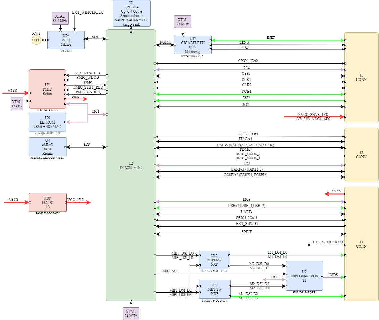
Main technical specifications
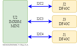
Form factor three 90-pins mezzanine connectors Hirose DF40C
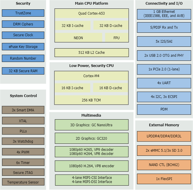
CPU Series: i.MX8M Mini (MIMX8MM6CVTKZAA)
Number of Cores/Core Processor: 4 x ARM Cortex A53, 1 x ARM Cortex-M4F
32 KB, 32 KB (instruction,data) L1 Cache
512 KB unified L2 Cache
Operating Frequency [Max] 1.6 GHz
RAM LPDDR4 16 GB, interface 32-bit (K4F6E3S4HM-MGCJ000)
FLASH eMMC FLASH 16 GB (THGAMRG7T13BAIL)
EEPROM I2C serial EEPROM 2 KB, Unique ID 48 bit (24AA025)
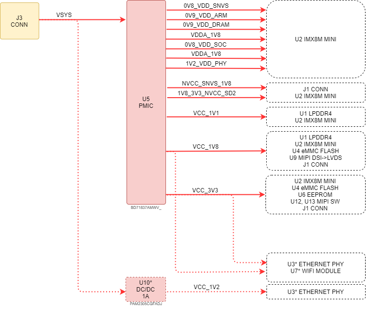
Power management IC PMIC (BD71847AMWV)
Other components WIFI (WF200C)
Ethernet PHY (KSZ9031)
MIPI® DSI→LVDS bridge (SN65DSI83ZQER)
3-lane high-speed MIPI compatible switch (NX3DV642GU,115)
Interfaces 1x PCIe
2x USB OTG 2.0
1x JTAG
1x Gigabit Ethernet (from gigabit PHY)
1x QSPI
2x ECSPI
4x SAI
1x SPDIF
1x SD
4x UART
4x I2C
1x LVDS (MIPI DSI → LVDS)
1x MIPI CSI
14x GPIO
Power supply voltage 3.5-5V FIXME
Power consumption TBD
Dimensions 55.2 х 30.1 mm


Block Diagram

boards:nms-cs-imx8mini:v2_ru:cardsom_imx8m_mini_v2_blockdiagram.drawio.png
Module block diagram


Power tree

boards:nms-cs-imx8mini:v2_ru:power_cardsom_imx8mini_v2.drawio.png
Module power tree


Mechanical Specifications

Board dimensions are: 55.2 х 30.1 mm.
Printed circuit of the board is made of 10 layers, some of them are ground planes, for disturbance rejection.

Module mechanical dimensions


Main Hardware Components

Component Location

Top View

Component Location. Top View


Component description on the board (Top side)
Designator P/N Description
U1 K4F6E3S4HM-MGCJ000 Memory LPDDR4
U2 MIMX8MM6CVTKZAA Processor i.MX8M Mini
U3* KSZ9031RN Ethernet PHY
U4 THGAMRG7T13BAIL e-MMC flash
U5 BD71847AMWV_ PMIC
U6 24AA025E48T-I/OT EEPROM
U7* WF200C Network Co-Processor Wi-Fi
U9 SN65DSI83ZQER MIPIDSI→LVDS bridge
U10* PAM2305CGFADJ DCDC converter 5V→1.2V
U12, U13 NX3DV642GU,115 3-lane high-speed MIPI compatible switch
* - absent in this version FIXME


Bottom View

On the bottom side of the board, the components are absent.

Processor

Figure 5 shows the functional modules in the i.MX8M MINI processor system.

boards:nms-cs-imx8mini:v2_ru:i.mx_8m_mini_diagram_old.drawio.png
i.MX8M Mini function modules


Interfaces

I2C

Three I2C interfaces are availbale on NMS-CS-IMX8MINI-V2.

boards:nms-cs-imx8mini:v2_ru:i2c_cardsom_imx8mini_v2.drawio.png
I2C interfaces


I2C Address Mapping
Device Address
MIPIDSI→2LVDS bridge 0x0101100
EEPROM 0x1010000
PMIC 0x1001000


I2C signal pinouts on J1-J3 connectors
Signal Name Pin(s) Direction Standard volgate (V) Description Connection
I2C2_SCL J2.32 in/out 3.3
PU 4.7 kΩ
General purpose I2C Bus clock line. U2.D10
I2C2_SDA J2.30 in/out 3.3
PU 4.7 kΩ
General purpose I2C Bus data line. U2.D9
I2C3_SCL J3.46 in/out 3.3
PU 4.7 kΩ
General purpose I2C Bus clock line. U2.E10
I2C3_SDA J3.42 in/out 3.3
PU 4.7 kΩ
General purpose I2C Bus data line. U2.F10
I2C4_SCL J1.17 in/out 3.3
PU 4.7 kΩ
General purpose I2C Bus clock line. U2.D13
I2C4_SDA J1.19 in/out 3.3
PU 4.7 kΩ
General purpose I2C Bus data line. U2.E13

where PU - pull-up resistor, PD - pull-down resistor.


Debugging/development interfaces

I2C

There is one I2C interface for communicating between processor and peripherals on NMS-CS-IMX8MINI-V2.

boards:nms-cs-imx8mini:v2_ru:cardsom_imx8mini_v2_i2c1.drawio.png
I2C1 interface


IMX8M_MINI I2C singnals
Signal name Pin(s) Direction Voltage standard Description
I2C1_SCL E9 in/out 3.3
PU 4.7 kΩ
General purpose I2C Bus clock line.
I2C1_SDA F9 in/out 3.3
PU 4.7 kΩ
General purpose I2C Bus data line.

where PU - pull-up resistor, PD - pull-down resistor.


RESET

boards:nms-cs-imx8mini:v2_ru:cardsom_imx8mini_resets.drawio.png
Reset signals


PMIC reset signals
Signal name Pin(s) Voltage standard(V) Circuit name Connection Description
PWRON U5.40 1.8
PU 100 kΩ
PWRON_B - Not used
POR U5.25 1.8
PU 10 kΩ
POR_B U2.B24, J1.24
1V8_POR_B U3.42, U4.K5
RTC_RESET U5.3 1.8
PU 100 kΩ
RTC_RESET U2.F4

where PU - pull-up resistor, PD - pull-down resistor.


CLK

boards:nms-cs-imx8mini:v2_ru:cardsom_imx8mini_v2_clk.drawio.png
Clock signals


J1 socket clock signals
Signal name Pin(s) Voltage Standart(V) Circuit Name Connection
GPIO1_IO00 1 LP_CLK U7.23 (through 0Ω )
NAND_DATA07/QSPIB_DATA3 35 CLK_I_N U2.J27
NAND_DATA06/QSPIB_DATA2 37 CLK_I_P U2.H27
NAND_CLE/QSPIB_SCLK 45 CLK_O_P U2.H26
NAND_CE2_B/QSPIB_SS0_B 47 CLK_O_N U2.J26
PCIE1_REF_CLKN 51 PCIE_REF_CLK_P U2.B21
PCIE1_REF_CLKP 53 PCIE_REF_CLK_N U2.A21


J3 socket clock signals
Signal Name Pin(s) Voltage Standart(V) Circuit name Connection
CSI_P2_DN0 84 EXT_LP_CLK U7.23 (through 0Ω )


External connectors

Connectors Location. Top View


Designator P/N Description
XW1 73412-0114 Microcoaxial connector for antenna
Component Location. Bottom View


Designator P/N Description
J1-J3 DF40C-90DP-0.4V Composite 90-pin mezzanine connector

connectors, alternatives

boards/nms-cs-imx8mini/v2_en/start.txt · Последнее изменение: 2022/06/22 11:42 — Roman Abakumov