| Form factor | three 90-pins mezzanine connectors Hirose DF40C |
|---|---|
| CPU | Series: i.MX8M Mini (MIMX8MM6CVTKZAA) |
| Number of Cores/Core Processor: 4 x ARM Cortex A53, 1 x ARM Cortex-M4F | |
| 32 KB, 32 KB (instruction,data) L1 Cache | |
| 512 KB unified L2 Cache | |
| Operating Frequency [Max] 1.6 GHz | |
| RAM | LPDDR4 16 GB, interface 32-bit (K4F6E3S4HM-MGCJ000) |
| FLASH | eMMC FLASH 16 GB (THGAMRG7T13BAIL) |
| EEPROM | I2C serial EEPROM 2 KB, Unique ID 48 bit (24AA025) |
| Power management IC | PMIC (BD71847AMWV) |
| Other components | WIFI (WF200C) |
| Ethernet PHY (KSZ9031) | |
| MIPI® DSI→LVDS bridge (SN65DSI83ZQER) | |
| 3-lane high-speed MIPI compatible switch (NX3DV642GU,115) | |
| Interfaces | 1x PCIe |
| 2x USB OTG 2.0 | |
| 1x JTAG | |
| 1x Gigabit Ethernet (from gigabit PHY) | |
| 1x QSPI | |
| 2x ECSPI | |
| 4x SAI | |
| 1x SPDIF | |
| 1x SD | |
| 4x UART | |
| 4x I2C | |
| 1x LVDS (MIPI DSI → LVDS) | |
| 1x MIPI CSI | |
| 14x GPIO | |
| Power supply voltage | 3.5-5V  |
| Power consumption | TBD |
| Dimensions | 55.2 х 30.1 mm |
Инструменты пользователя
Боковая панель
Содержание
NMS-CS-IMX8MINI v2 ds-en

System on Module NMS-CS-IMX8MINI-V2 is based on an ARM archtecture proccessor NXP i.MX8M Mini.
Technical Specifications
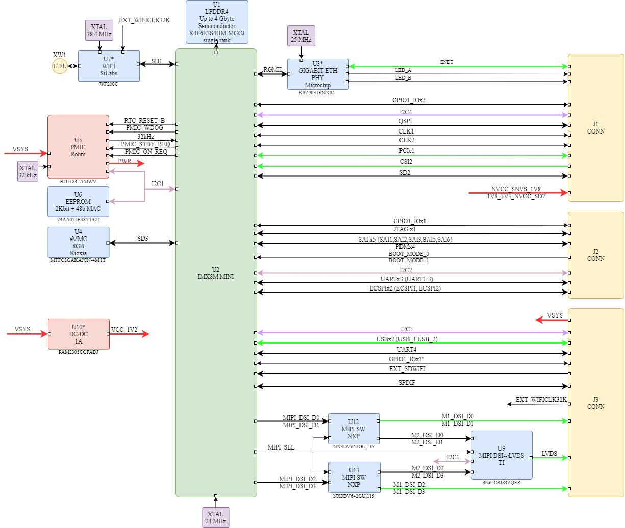
Block Diagram
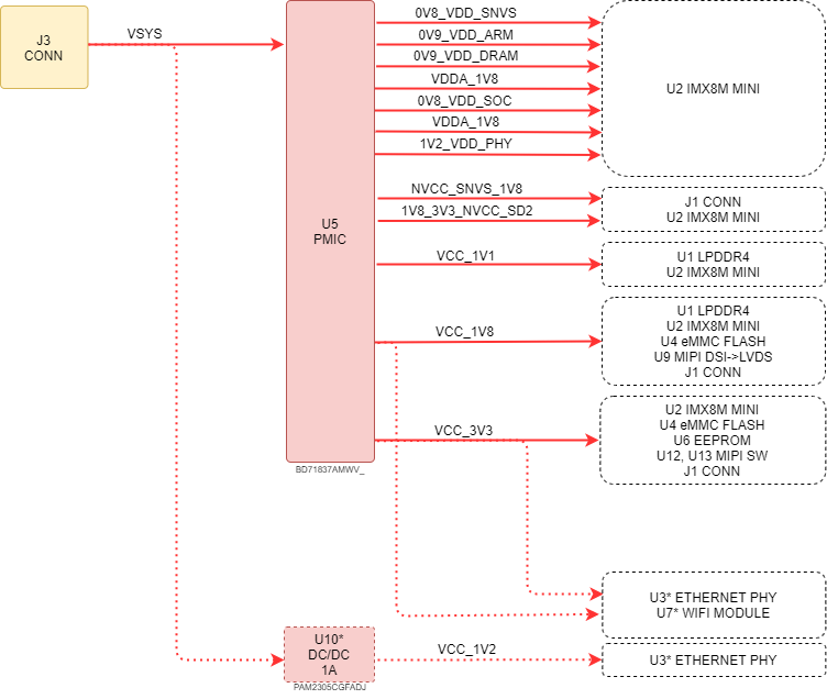
Power tree
Mechanical Specifications
Board dimensions are: 55.2 х 30.1 mm.
Printed circuit of the board is made of 10 layers, some of them are ground planes, for disturbance rejection.
Main Hardware Components
Component Location
Top View
| Designator | P/N | Description |
|---|---|---|
| U1 | K4F6E3S4HM-MGCJ000 | Memory LPDDR4 |
| U2 | MIMX8MM6CVTKZAA | Processor i.MX8M Mini |
| U3* | KSZ9031RN | Ethernet PHY |
| U4 | THGAMRG7T13BAIL | e-MMC flash |
| U5 | BD71847AMWV_ | PMIC |
| U6 | 24AA025E48T-I/OT | EEPROM |
| U7* | WF200C | Network Co-Processor Wi-Fi |
| U9 | SN65DSI83ZQER | MIPIDSI→LVDS bridge |
| U10* | PAM2305CGFADJ | DCDC converter 5V→1.2V |
| U12, U13 | NX3DV642GU,115 | 3-lane high-speed MIPI compatible switch |
* - absent in this version  |
||
Bottom View
On the bottom side of the board, the components are absent.
Processor
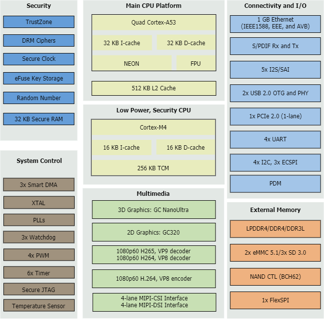
Figure 5 shows the functional modules in the i.MX8M MINI processor system.
Interfaces
I2C
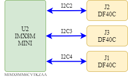
Three I2C interfaces are availbale on NMS-CS-IMX8MINI-V2.
| Device | Address |
|---|---|
| MIPIDSI→2LVDS bridge | 0x0101100 |
| EEPROM | 0x1010000 |
| PMIC | 0x1001000 |
| Signal Name | Pin(s) | Direction | Standard volgate (V) | Description | Connection |
|---|---|---|---|---|---|
| I2C2_SCL | J2.32 | in/out | 3.3 PU 4.7 kΩ | General purpose I2C Bus clock line. | U2.D10 |
| I2C2_SDA | J2.30 | in/out | 3.3 PU 4.7 kΩ | General purpose I2C Bus data line. | U2.D9 |
| I2C3_SCL | J3.46 | in/out | 3.3 PU 4.7 kΩ | General purpose I2C Bus clock line. | U2.E10 |
| I2C3_SDA | J3.42 | in/out | 3.3 PU 4.7 kΩ | General purpose I2C Bus data line. | U2.F10 |
| I2C4_SCL | J1.17 | in/out | 3.3 PU 4.7 kΩ | General purpose I2C Bus clock line. | U2.D13 |
| I2C4_SDA | J1.19 | in/out | 3.3 PU 4.7 kΩ | General purpose I2C Bus data line. | U2.E13 |
where PU - pull-up resistor, PD - pull-down resistor.
Debugging/development interfaces
I2C
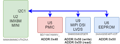
There is one I2C interface for communicating between processor and peripherals on NMS-CS-IMX8MINI-V2.
| Signal name | Pin(s) | Direction | Voltage standard | Description |
|---|---|---|---|---|
| I2C1_SCL | E9 | in/out | 3.3 PU 4.7 kΩ | General purpose I2C Bus clock line. |
| I2C1_SDA | F9 | in/out | 3.3 PU 4.7 kΩ | General purpose I2C Bus data line. |
where PU - pull-up resistor, PD - pull-down resistor.
RESET
| Signal name | Pin(s) | Voltage standard(V) | Circuit name | Connection | Description |
|---|---|---|---|---|---|
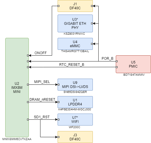
| PWRON | U5.40 | 1.8 PU 100 kΩ | PWRON_B | - | Not used |
| POR | U5.25 | 1.8 PU 10 kΩ | POR_B | U2.B24, J1.24 | |
| 1V8_POR_B | U3.42, U4.K5 | ||||
| RTC_RESET | U5.3 | 1.8 PU 100 kΩ | RTC_RESET | U2.F4 |
where PU - pull-up resistor, PD - pull-down resistor.
CLK
| Signal name | Pin(s) | Voltage Standart(V) | Circuit Name | Connection |
|---|---|---|---|---|
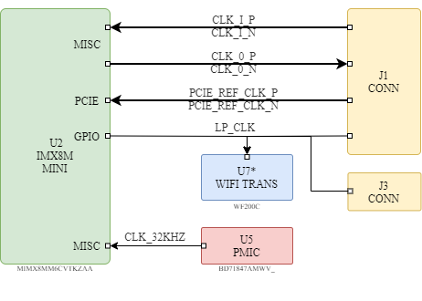
| GPIO1_IO00 | 1 | LP_CLK | U7.23 (through 0Ω ) | |
| NAND_DATA07/QSPIB_DATA3 | 35 | CLK_I_N | U2.J27 | |
| NAND_DATA06/QSPIB_DATA2 | 37 | CLK_I_P | U2.H27 | |
| NAND_CLE/QSPIB_SCLK | 45 | CLK_O_P | U2.H26 | |
| NAND_CE2_B/QSPIB_SS0_B | 47 | CLK_O_N | U2.J26 | |
| PCIE1_REF_CLKN | 51 | PCIE_REF_CLK_P | U2.B21 | |
| PCIE1_REF_CLKP | 53 | PCIE_REF_CLK_N | U2.A21 |
| Signal Name | Pin(s) | Voltage Standart(V) | Circuit name | Connection |
|---|---|---|---|---|
| CSI_P2_DN0 | 84 | EXT_LP_CLK | U7.23 (through 0Ω ) |
External connectors
| Designator | P/N | Description |
|---|---|---|
| XW1 | 73412-0114 | Microcoaxial connector for antenna |
| Designator | P/N | Description |
|---|---|---|
| J1-J3 | DF40C-90DP-0.4V | Composite 90-pin mezzanine connector |


