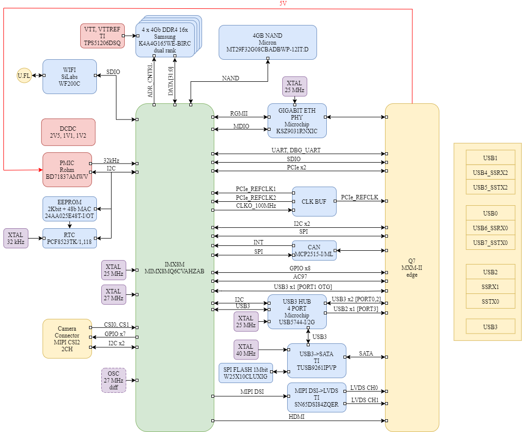

Main technical specifications
| Form factor | μQseven |
|---|---|
| CPU | Series: i.MX 8MQuad (MIMX8MQ6CVAHZAB) |
| Number of Cores/Core Processor: 4 x ARM Cortex A53@ 1.5 GHz, 1 x ARM Cortex M4@266 MHz | |
| 32 KB, 16 KB L1 Cache | |
| 1 MB unified L2 Cache | |
| Operating Frequency [Max]: 1.3 GHz | |
| RAM | Dual rank DDR4 2 GB, interface 32-bit K4A4G165WE) |
| FLASH | NAND 4GB (4Gbit x 8) (MT29F32) |
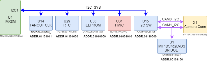
| EEPROM | I2C serial EEPROM 256 byte, Unique ID (24AA025) |
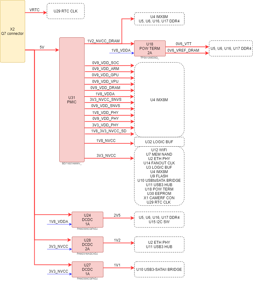
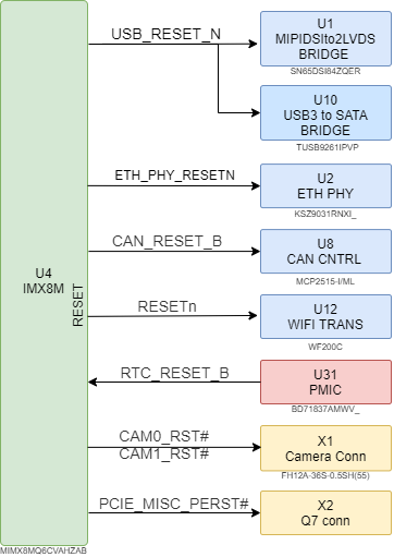
| Power management IC | PMIC (BD71837) |
| Other components | RTC (PCF8523TK) |
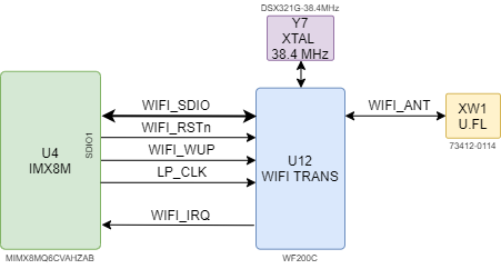
| WIFI (WF200C) | |
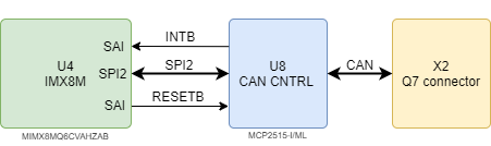
| CAN controller (MCP2515-I) | |
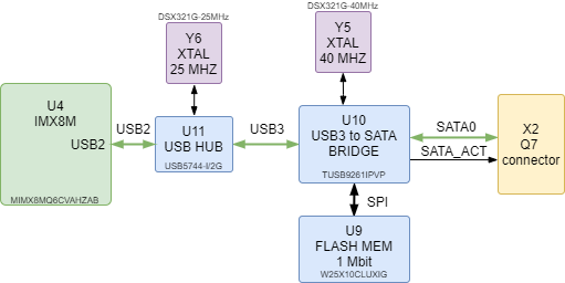
| USB3.0→SATA bridge(TUSB9261IPVP) | |
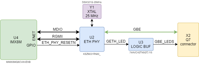
| Ethernet PHY KSZ9031 | |
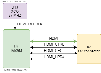
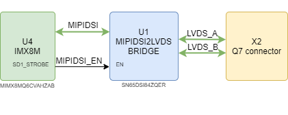
| MIPI® DSI→LVDS bridge SN65DSI84ZQER | |
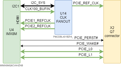
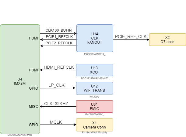
| Interfaces | PCIe 1x + PCIe 1x + PCIe refclk |
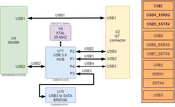
| 1х USB 3.0 OTG | |
| 2х USB 3.0 (USB 3.0 HUB) | |
| 1x USB 2.0 (USB 3.0 HUB) | |
| 1x SATA (USB3.0→SATA bridge) | |
| 1x Gigabit Ethernet (from gigabit PHY) | |
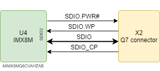
| 1x SDIO | |
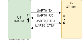
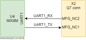
| 1x UART + 1x debug UART | |
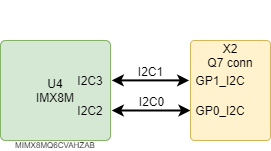
| 2x I2C | |
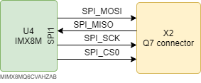
| 1x SPI | |
| 1x CAN | |
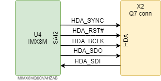
| 1x audio AC97 | |
| LVDS 2x (MIPI DSI → LVDS 2 channels) | |
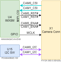
| MIPI CSI2 (external connector, CSI2 x4 + CSI2 x2 + GPIO x7 + I2C x2) | |
| Power supply voltage | +5 Volt |
| Power consumption | TBD |
| Dimensions | 70×40 mm |