

System on Module SOM-IMX8M_UQ7 is based on the NXP i.MX8M applications processor with ARM Cortex-A53 and Cortex-M4 architecture.

| Form factor | μQseven |
|---|---|
| CPU | Series: i.MX 8MQuad (MIMX8MQ6CVAHZAB) |
| Number of Cores/Core Processor: 4 x ARM Cortex A53@ 1.5 GHz, 1 x ARM Cortex M4@266 MHz | |
| 32 KB, 16 KB L1 Cache | |
| 1 MB unified L2 Cache | |
| Operating Frequency [Max]: 1.3 GHz | |
| RAM | Dual rank DDR4 2 GB, interface 32-bit K4A4G165WE) |
| FLASH | NAND 4GB (4Gbit x 8) (MT29F32) |
| EEPROM | I2C serial EEPROM 256 byte, Unique ID (24AA025) |
| Power management IC | PMIC (BD71837) |
| Other components | RTC (PCF8523TK) |
| WIFI (WF200C) | |
| CAN controller (MCP2515-I) | |
| USB3.0→SATA bridge(TUSB9261IPVP) | |
| Ethernet PHY KSZ9031 | |
| MIPI® DSI→LVDS bridge SN65DSI84ZQER | |
| Interfaces | PCIe 1x + PCIe 1x + PCIe refclk |
| 1х USB 3.0 OTG | |
| 2х USB 3.0 (USB 3.0 HUB) | |
| 1x USB 2.0 (USB 3.0 HUB) | |
| 1x SATA (USB3.0→SATA bridge) | |
| 1x Gigabit Ethernet (from gigabit PHY) | |
| 1x SDIO | |
| 1x UART + 1x debug UART | |
| 2x I2C | |
| 1x SPI | |
| 1x CAN | |
| 1x audio AC97 | |
| LVDS 2x (MIPI DSI → LVDS 2 channels) | |
| MIPI CSI2 (external connector, CSI2 x4 + CSI2 x2 + GPIO x7 + I2C x2) | |
| Power supply voltage | +5 Volt |
| Power consumption | TBD |
| Dimensions | 70×40 mm |
Board dimensions are: 70 х 40 mm.
Printed circuit of the board is made of 12 layers, some of them are ground planes, for disturbance rejection.


| Designator | P/N | Description |
|---|---|---|
| U1 | SN65DSI84ZQER | MIPIDSI→2LVDS bridge |
| U2 | KSZ9031RNXI_ | Ethernet PHY |
| U3 | 74AVCH2T45GT,115 | Dual-bit, dual-supply voltage level translator/transceiver |
| U4 | MIMX8MQ6CVAHZAB | Processor |
| U5 | K4A4G165WE-BIRC | DDR4 SDRAM |
| U6 | K4A4G165WE-BIRC | DDR4 SDRAM |
| U10 | TUSB9261IPVP | USB3.0→SATA bridge |
| U11 | USB5744-I/2G | USB3 HUB |
| U14 | PI6CDBL401BZHI_ | 4-Output Low Power PCIE GEN1-2-3 Buffer |
| U28 | PAM2316AGCADJ | DCDC Converter 5V→1.2V |
| U29 | PCF8523TK/1,118 | RTC |
| U31 | BD71837AMWV_ | PMIC |
| U32 | 74AVCH2T45GT,115 | Dual-bit, dual-supply voltage level translator/transceiver |

| Designator | P/N | Description |
|---|---|---|
| U7 | MT29F32G08CBADBWP-12IT:D | NAND Flash Memory |
| U8 | MCP2515-I/ML | CAN Controller |
| U9 | W25X10CLUXIG | Flash Memory 1Mb |
| U12 | WF200C | Wi-Fi Network Co-Processor |
| U15 | PCA9540BGD,125 | 2-channel I2C-bus multiplexer |
| U16 | K4A4G165WE-BIRC | DDR4 SDRAM |
| U17 | K4A4G165WE-BIRC | DDR4 SDRAM |
| U18 | TPS51206DSQ_ | DDR Termination Regulator |
| U24 | PAM2305CGFADJ | DCDC Converter 5V→2.5V |
| U27 | PAM2305CGFADJ | DCDC Converter 5V→1.1V |
| U30 | 24AA025E48T-I/OT | 2K I2C Serial EEPROM |
The i.MX 8M Quad processor feature advanced implementation of a quad Arm®Cortex®-A53 core, which operates at speeds of up to 1.5 GHz. A general purpose Cortex®-M4 core processor is for low-power processing. The DRAM controller supports 32-bit/16-bit LPDDR4, DDR4, and DDR3L memory. There are a number of other interfaces for connecting peripherals, such as WLAN, Bluetooth, GPS, displays, and camera sensors. The i.MX 8M Quad and i.MX 8M Dual processors have hardware acceleration for video playback up to 4K, and can drive the video outputs up to 60 fps.
Figure 6 shows the functional modules in the i.MX 8M Quad processor system.

SOM-IMX8M_UQ7 is available with dual rank Samsung DDR4 memory K4A4G165.
The 4Gb DDR4 SDRAM is organized as a 32Mbit x 16 I/Os x 8banks device.
This synchronous device achieves high speed double-data-rate transfer rates of up to 2666Mb/sec/pin (DDR4-2666) for general applications.
All of the control and address inputs are synchronized with a pair of externally supplied differential clocks.
The DDR4 device operates with a single 1.2V (1.14V~1.26V) power supply, 1.2V (1.14V~1.26V) VDDQ and 2.5V (2.375V~2.75V) VPP.
SOM-IMX8M_UQ7 has Micron NAND Flash device MT29F32 on board.
Flash memory use a highly multiplexed 8-bit bus to transfer data, addresses, and instructions.
This flash device additionally includes a synchronous data interface forhigh-performance I/O operations.
When the synchronous interface is active, WE# becomes CLK and RE# becomes W/R#. Data transfers include a bidirectional data strobe(DQS).
SOM-IMX8M_UQ7 has Microchip Technology Inc. 2 Kbit I2C Serial Electrically Erasable PROM (EEPROM) 24AA025 on board.
The EEPROM has a page write capability for up to 16 bytes of data.
The device is organized as two blocks of 128 x 8-bit memory with a 2-wire serial interface.
The SOM-IMX8M_UQ7 features ROHM BD71837 as a Power Management Integrated circuit (PMIC) designed specifically for use with NXP’s i.MX8M series of application processors.
The PMIC regulates all power rails required on SOM from a single power supply with 5V.
The PMIC is fully programmable via the I2C interface and associated register map.
Software reset signal (WDOG_B) is used to perform a complete reset of the SOM-IMX8M_UQ7 module.
Reset button is installed on the motherboard for a complete reboot.
SOM-IMX8M_UQ7 has NXP Real-Time Clock (RTC) PCF8523 on board.
Data is transferred serially via the I2C-bus with a maximum data rate of 1000 kbit/s.
Alarm and timer functions are available with the possibility to generate a wake-up signal on an interrupt pin.
The PCF8523 has a backup battery switch-over circuit, which detects power failures and automatically switches to the battery supply when a power failure occurs.
SOM-IMX8M_UQ7 has Silicon Labs Ultra Low Power Wi-Fi transceiver or network co-processor (NCP) WF200С on board.
WF200 is a Wi-Fi network co-processor low energy, and low cost, with two antenna ports, Crystal Oscillator, One Time Programmable Memory,
and several GPIOs for interfacing with multi-protocol and RF Front End Module controls.
SDIO interface using to communicate with the external host controller.
SOM-IMX8M_UQ7 has Microchip CAN controller MCP2515 on board.
The MCP2515 is used standard serial peripheral interface (SPI) to communicate with the i.MX8M processor.
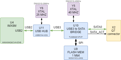
SOM-IMX8M_UQ7 has an ARM Cortex M3 microcontroller based USB 3.0 to serial ATA bridge TUSB9261 on board.
It provides the necessary hardware and firmware to implement a USB attached SCSI protocol (UASP)-compliant mass storage device suitable for bridging hard disk drives (HDD),
solid state disk drives (SSD), optical drives, and other compatible SATA 1.5-Gbps or SATA 3.0-Gbps devices to a USB 3.0 bus.
A KDS 40 MHz crystal resonator DSX321G is used as the primary clock source.
The Winbond SPI flash device W25X10 contains firmware that loads into TUSB9261 after RESET.
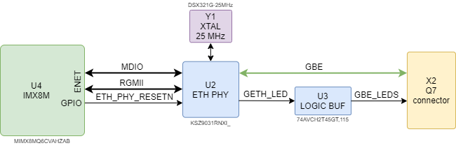
SOM-IMX8M_UQ7 is available with completely integrated triple-speed (10BASE-T/100BASE-TX/1000BASE-T) Micrel Ethernet physicallayer
transceiver KSZ9031 for transmission and reception of data on standard CAT-5 unshielded twisted pair (UTP) cable.
The KSZ9031 provides the Reduced Gigabit Media Independent Interface (RGMII) for direct connection to RGMII MACs in Gigabit Ethernet
processors and switches for data transfer at 10/100/1000 Mbps.
SOM-IMX8M_UQ7 has Texas Instruments single channel DSI to dual-link LVDS bridge SN65DSI84 on board.
The SN65DSI84 features a single-channel MIPI D-PHY receiver front-end configuration with 4 lanes per channel operating at 1 Gbps per lane; a maximum input bandwidth of 4 Gbps.
It has a range of power management features including lowswing LVDS outputs, and the MIPI defined ultra-low power state (ULPS) support.
The SN65DSI84 is well suited for WUXGA 1920 x 1200 at 60 frames per second, with up to 24 bits-perpixel.
Partial line buffering is implemented to accommodate the data stream mismatch between the DSI and LVDS interfaces.
The bridge decodes MIPI DSI and converts the formatted video data stream to a FlatLink compatible LVDS output.
It is offering a DualLink LVDS, Single-Link LVDS interface with four data lanes per link.

| Designator | P/N | Description |
|---|---|---|
| X1 | FH12A-36S-0.5SH(55) | FPC / FFC camera connector |
| X2 | MXM-II | MXM-II format connector for connecting with a motherboard |
| XW1 | 73412-0114 | Microcoaxial WIFI Connector |
SOM-IMX8M_UQ7 has one MXM2 connector (X2 slot) with 230 contacts in 0.5 mm increments for communication with the motherboard Q7_Base.
The pin assignment see in Appendix 1.
SOM-IMX8M_UQ7 has one HIROSE FPC/FFC connector FH12A-36S-0.5SH (55) for connecting camera.
SOM-IMX8M_UQ7 has one MOLEX micro-coaxial connector 73412-0114 for connecting a WIFI antenna.
Two MIPI CSI interfaces are available on SOM-IMX8M_UQ7.
MIPI CSI interface provides transfering image data directly from the camera or sensor module to the processor.
This standard also specifies an interface for a camera configuration via I²C, namely CCI (Camera Control Interface).
With MIPI CSI-2, the image data are transferred serially through individual lanes.
| Signal Name | Pin(s) | Direction | Voltage standard | Description | Connection |
|---|---|---|---|---|---|
| CAM_PWR | 1 | 3V3 | Power. | ||
| CAM_PWR | 2 | 3V3 | Power. | ||
| CAM0_CSI_D0+ | 3 | out | CSI2 Camera 0 Data Lane 0. | U4.B23 | |
| CAM0_CSI_D0- | 4 | out | U4.A23 | ||
| GND | 5 | Power. | |||
| CAM0_CSI_D1+ | 6 | out | CSI2 Camera 0 Data Lane 1. | U4.D22 | |
| CAM0_CSI_D1- | 7 | out | U4.C22 | ||
| GND | 8 | Power. | |||
| CAM0_CSI_D2+ | 9 | out | CSI2 Camera 0 Data Lane 2. | U4.C23 | |
| CAM0_CSI_D2- | 10 | out | U4.B24 | ||
| CAM0_RST# | 11 | in | 1V8 | Camera 0 Reset. | U4.P7 |
| CAM0_CSI_D3+ | 12 | out | CSI2 Camera 0 Data Lane 3. | U4.D21 | |
| CAM0_CSI_D3- | 13 | out | U4.C21 | ||
| GND | 14 | Power. | |||
| CAM0_CSI_CLK+ | 15 | out | CSI2 Camera 0 Differential Clock. | U4.B22 | |
| CAM0_CSI_CLK- | 16 | out | U4.A22 | ||
| GND | 17 | Power. | |||
| CAM0_I2C_CLK | 18 | in | 1V8 PU 2k2Ω | Camera 0 Control I2C Interface, CLK. | U15.5 |
| CAM0_I2C_DAT | 19 | in/out | 1V8 PU 2k2Ω | Camera 0 Control I2C Interface, DATA. | U15.4 |
| CAM0_ENA# | 20 | in | 1V8 | Camera 0 Enable. | U4.T7 |
| MCLK | 21 | in | Master Clock. | U4.K7 | |
| CAM1_ENA# | 22 | in | 1V8 | Camera 1 Enable. | U4.P5 |
| CAM1_I2C_CLK | 23 | out | 1V8 PU 2k2Ω | Camera 1 Control I2C Interface, CLK. | U15.8 |
| CAM1_I2C_DAT | 24 | out | 1V8 PU 2k2Ω | Camera 1 Control I2C Interface, DATA. | U15.7 |
| GND | 25 | Power | |||
| CAM1_CSI_CLK+ | 26 | out | CSI2 Camera 1 Differential Clock. | U4.B19 | |
| CAM1_CSI_CLK- | 27 | out | U4.A19 | ||
| GND | 28 | Power. | |||
| CAM1_CSI_D0+ | 29 | out | CSI2 Camera 1 Data Lane 0. | U4.D20 | |
| CAM1_CSI_D0- | 30 | out | U4.C20 | ||
| CAM1_RST# | 31 | in | 1V8 | Camera 1 Reset. | U4.N6 |
| CAM1_CSI_D1+ | 32 | out | CSI2 Camera 1 Data Lane 1. | U4.B20 | |
| CAM1_CSI_D1- | 33 | out | U4.A20 | ||
| GND | 34 | Power. | |||
| CAM0_GPIO | 35 | in/out | 1V8 | GPIO for Camera 0. | U4.P4 |
| CAM1_GPIO | 36 | in/out | 1V8 | GPIO for Camera 1. | U4.N5 |
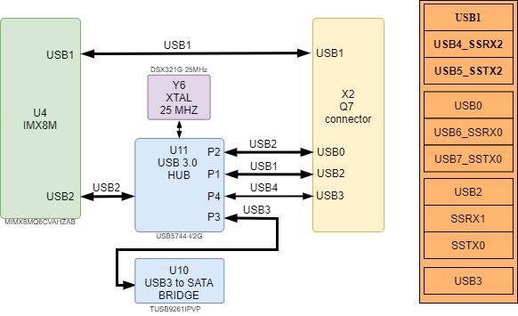
Four USB interfaces are available on SOM-IMX8M_UQ7:
| Signal Name | Pin(s) | Direction | Voltage standard | Description | Connection |
|---|---|---|---|---|---|
| USB_P0+ | 96 | in/out | Universal Serial Bus Port #0 differential pair. | U11.8 | |
| USB_P0- | 94 | U11.9 | |||
| USB_P1+ | 95 | in/out | Universal Serial Bus Port #1 differential pair. | U4.A14 | |
| USB_P1- | 93 | U4.B14 | |||
| USB_P2+ | 90 | in/out | Universal Serial Bus Port #2 differential pair. | U11.1 | |
| USB_P2- | 88 | U11.2 | |||
| USB_P3+ | 89 | in/out | Universal Serial Bus Port #3 differential pair. | U11.17 | |
| USB_P3- | 87 | U11.18 | |||
| USB_P4+/USB_SSRX2+ | 84 | in/out | USB Super Speed Port #2 receive differential pair. | U4.A12 | |
| USB_P4-/USB_SSRX2- | 82 | U4.B12 | |||
| USB_P5+/USB_SSTX2+ | 83 | out | USB Super Speed Port #2 transmit differential pair, AC coupled 0u1F. | U4.A13 | |
| USB_P5-/USB_SSTX2- | 81 | U4.B13 | |||
| USB_P6+/USB_SSRX0+ | 78 | in/out | USB Super Speed Port #0 receive differential pair. | U11.13 | |
| USB_P6-/USB_SSRX0- | 76 | U11.14 | |||
| USB_P7+/USB_SSTX0+ | 77 | in/out | USB Super Speed Port #0 transmit differential pair, AC coupled 0u1F. | U11.10 | |
| USB_P7-/USB_SSTX0- | 75 | U11.11 | |||
| USB_SSRX1+ | 132 | in | USB Super Speed Port #1 receive differential pair. | U11.3 | |
| USB_SSRX1- | 134 | U11.4 | |||
| USB_SSTX1+ | 144 | out | USB Super Speed Port #1 transmit differential pair, AC coupled 0u1F. | U11.6 | |
| USB_SSTX1- | 146 | U11.7 | |||
| USB_0_1_OC# | 86 | out | 3V3 PU 10kΩ | USB Over Current Detect Input. This pin used for overcurrent detection of USB Port#0 and #1. | U4.J4 |
| USB_2_3_OC# | 85 | out | 3V3 PU 10kΩ | USB Over Current Detect Input. This pin has to be used for overcurrent detection of USB Ports #2 and/or #3. | U4.E1 |
| USB_4_5_OC# | 80 | out | 3V3 PU 10kΩ | USB Over Current Detect Input. This pin used for overcurrent detection of USB Port #4 and/or #5. | U4.H1 |
| USB_6_7_OC# | 79 | in | 3V3 PU 10kΩ | USB Over Current Detect Input. This pin used for overcurrent detection of USB Port #6 and/or #7. | U4.K1 |
| USB_VBUS | 91 | in | 3V3 | USB Client mode Power Input. | U4.D14 |
| USB_ID | 92 | in | 3V3 PU 10kΩ | USB ID Input. USB Port #1 has set to work in Host mode. | U4.C14 |
| USB_OTG_PEN | 56 | out | 3V3 | USB Power enable pin for USB Port 1. | U4.L1 |
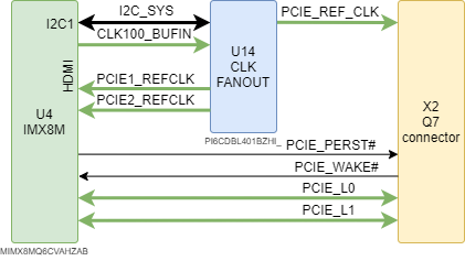
Two PCIe interfaces are available on SOM-IMX8M_UQ7.
| Signal Name | Pin(s) | Direction | Voltage standard | Description | Connection |
|---|---|---|---|---|---|
| PCIE0_TX+ | 179 | out | PCI Express channel #0, Transmitting Input Differential pair, AC coupled 0u1F. | U4.J25 | |
| PCIE0_TX- | 181 | U4.J24 | |||
| PCIE0_RX+ | 180 | in | PCI Express channel #0, Receiving Output Differential pair. | U4.H25 | |
| PCIE0_RX- | 182 | U4.H24 | |||
| PCIE1_TX+ | 173 | out | PCI Express channel #1, Transmitting Input Differential pair, AC coupled 0u1F. | U4.E25 | |
| PCIE1_TX- | 175 | U4.E24 | |||
| PCIE1_RX+ | 174 | in | PCI Express channel #1, Receiving Output Differential pair. | U4.D25 | |
| PCIE1_RX- | 176 | U4.D24 | |||
| PCIE2_TX+ | 167 | out | PCI Express channel #2, Transmitting Input Differential pair. | Not used. | |
| PCIE2_TX- | 169 | ||||
| PCIE2_RX+ | 168 | in | PCI Express channel #2, Receiving Output Differential pair. | Not used. | |
| PCIE2_RX- | 170 | ||||
| PCIE3_TX+ | 161 | out | PCI Express channel #3, Transmitting Input Differential pair. | Not used. | |
| PCIE3_TX- | 163 | ||||
| PCIE3_RX+ | 162 | in | PCI Express channel #3, Receiving Output Differential pair. | Not used. | |
| PCIE3_RX- | 164 | ||||
| PCIE_CLK_REF+ | 155 | in | PCI Express Reference Clock for channel 0 to 3, Differential Pair. | U14.22 | |
| PCIE_CLK_REF- | 157 | U14.23 | |||
| PCIE_WAKE# | 156 | in | 3V3 PU 10kΩ | Wake-up signal of the QSeven module system. | U4.K5 |
| PCIE_RST# | 158 | out | 3V3 | Reset signal for devices on the motherboard. | U4.K4 |
SOM-IMX8M_UQ7 has Pericom Semiconductor 4-output low power PCIE GEN1-2-3 buffer PI6CDBL401B with integrated output terminations providing Zo=100Ω.
The device has an output control function via the I2C-bus.
Device Address: 0x1101011.
| Signal Name | Pin(s) | Direction | Voltage standard | Description | Connection |
|---|---|---|---|---|---|
| SATA0_TX+ | 29 | out | Serial ATA Channel #0 Transmit differential pair, AC coupled 0u1F. | U10.57 | |
| SATA0_TX- | 31 | U10.56 | |||
| SATA0_RX+ | 35 | in | Serial ATA Channel #0 Receive differential pair, AC coupled 0u1F. | U10.60 | |
| SATA0_RX- | 37 | U10.59 | |||
| SATA_ACT# | 33 | out | 3V3 | Serial ATA Activity Led. | U10.2 |
| SATA1_TX+ | 30 | out | Serial ATA channel 1, Receive Input differential pair. | Not used. | |
| SATA1_TX- | 32 | ||||
| SATA1_RX+ | 36 | in | Serial ATA channel 1, Transmit Output differential pair. | Not used. | |
| SATA1_RX- | 38 |
One Gigabit Ethernet interface is available on SOM-IMX8M_UQ7.
The Ethernet interface supports triple speed 10/100/1000 Mbit/s Ethernet MAC (compliant with the IEEE802.3-2002 standard)
and compatibles with half- or full-duplex 10/100 Mbit/s Ethernet LANs and full-duplex gigabit Ethernet LANs.
| Signal Name | Pin(s) | Direction | Voltage standard | Description | Connection |
|---|---|---|---|---|---|
| GBE_MDI0+ | 12 | in/out | Media Dependent Interface (MDI) I/O differential pair #0. The MDI can operate in 1000, 100, and 10Mbit/sec modes. This signal pair is used for all modes. | U2.2 | |
| GBE_MDI0- | 10 | U2.3 | |||
| GBE_MDI1+ | 11 | in/out | Media Dependent Interface (MDI) I/O differential pair #1. The MDI can operate in 1000, 100, and 10Mbit/sec modes. This signal pair is used for all modes. | U2.5 | |
| GBE_MDI1- | 9 | U2.6 | |||
| GBE_MDI2+ | 6 | in/out | Media Dependent Interface (MDI) I/O differential pair #2. The MDI can operate in 1000, 100, and 10Mbit/sec modes. This signal pair is only used for 1000Mbit/sec Gigabit Ethernet mode. | U2.7 | |
| GBE_MDI2- | 4 | U2.8 | |||
| GBE_MDI3+ | 5 | in/out | Media Dependent Interface (MDI) I/O differential pair #3. The MDI can operate in 1000, 100, and 10Mbit/sec modes. This signal pair is only used for 1000Mbit/sec Gigabit Ethernet mode. | U2.9 | |
| GBE_MDI3- | 3 | U2.10 | |||
| GBE_ACT# | 14 | out | 3V3 | Ethernet controller activity indicator. | U3.7 |
| GBE_LINK# | 13 | out | 3V3 | Ethernet controller link indicator. | U3.6 |
| GBE_LINK100# | 7 | out | 3V3 | Ethernet controller 100Mbps link indicator. | Not used. |
| GBE_LINK1000# | 8 | out | 3V3 | Ethernet controller 1Gbps link indicator. | U3.6 |
| GBE_CTREF | 15 | out | Reference voltage for Ethernet channel 0 magnetics center tap. | Not used. |
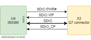
One SDIO (SD2) interface is available on SOM-IMX8M_UQ7.
Supports SD/SDIO standard, up to version 3.0, MMC standard, up to version 5.0, 1-bit / 4-bit SD and SDIO (SD2) modes,
1-bit / 4-bit / 8-bit MMC (SD1) mode.
| Signal Name | Pin(s) | Direction | Voltage standard | Description | Connection |
|---|---|---|---|---|---|
| SDIO_CD# | 43 | in/out | 3V3 PU 10kΩ | SDIO Card Detect. This signal indicates when a SDIO/MMC card is present. | U4.L21 |
| SDIO_CLK | 42 | out | 3V3 | SDIO Clock. With each cycle of this signal a one-bit transfer on the command and each data line occurs. | U4.L22 |
| SDIO_CMD | 45 | in/out | 3V3 | SDIO Command/Response line. This signal is used for card initialization and for command transfers. | U4.M22 |
| SDIO_LED | 44 | out | 3V3 | SDIO LED. Used to drive an external LED to indicate when transfers occur on the bus. | Not used. |
| SDIO_WP | 46 | in/out | 3V3 | SDIO Write Protect. This signal denotes the state of the write-protect tab on SD cards. | U4.M21 |
| SDIO_PWR# | 47 | out | 3V3 | SDIO Power Enable. This signal is used to enable the power being supplied to a SD/MMC card device. | U4.R22 |
| SDIO_DAT[0÷7] | 48-51 | in/out | 3V3 | SDIO data bus. SDIO_DAT0 signal is used for all communication modes. SDIO_DAT[1 ÷ 3] signals are required for 4-bit SDIO communication modes. SDIO_DAT[4÷7] not used. | SDIO_DAT[0÷3] - [U4.N22 U4.N21 U4.P22 U4.P21] |
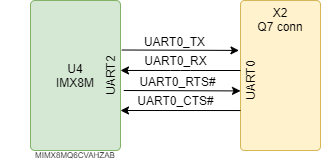
One UART (UART2) interface is available on SOM-IMX8M_UQ7.
The Universal Asynchronous Receiver/Transmitter (UART) provides serial communication capability with external devices through a level converter.
| Signal Name | Pin(s) | Direction | Voltage standard | Description | Connection |
|---|---|---|---|---|---|
| UART0_TX | 171 | out | 3V3 | UART Interface, Serial data Transmit line. | U4.D6 |
| UART0_RX | 177 | in | 3V3 PU 10kΩ | UART Interface, Serial data Receive line. | U4.B6 |
| UART0_RTS# | 172 | out | 3V3 | UART Interface, Handshake signal, Request to Send line. | U4.D7 |
| UART0_CTS# | 178 | in | 3V3 | UART Interface, Handshake signal, Clear to Send line. | U4.C6 |
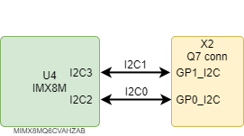
Two I2C interfaces are available on SOM-IMX8M_UQ7.
I2C is a two-wire, bidirectional serial bus that provides a simple, efficient method of data exchange, minimizing the interconnection between devices.
| Signal Name | Pin(s) | Direction | Voltage standard | Description | Connection |
|---|---|---|---|---|---|
| SMB_CLK | 60 | in/out | 3V3 PU 4k7Ω | SM Bus control clock line for System Management. | U4.G8 |
| SMB_DAT | 62 | in/out | 3V3 PU 4k7Ω | SM Bus control data line for System Management. | U4.E9 |
| SMB_ALERT# | 64 | in/out | 3V3 PU 4k7Ω | SM Bus Alert line for System Management. | Not used. |
| GP0_I2C_CLK | 66 | in/out | 3V3 PU 4k7Ω | General purpose I2C Bus clock line. | U4.G7 |
| GP0_I2C_DAT | 68 | in/out | 3V3 PU 4k7Ω | General purpose I2C Bus data line. | U4.F7 |
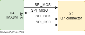
One SPI interface is available on SOM-IMX8M_UQ7 (master or slave mode).
| Signal Name | Pin(s) | Direction | Voltage standard | Description | Connection |
|---|---|---|---|---|---|
| SPI_MOSI | 199 | out | 3V3 | SPI Master Out Slave In (module QSeven → SPI devices (motherboard)). | U4.A4 |
| SPI_MISO | 201 | in | 3V3 | SPI Master In Slave Out ( SPI devices(motherboard)→ module QSeven). | U4.B4 |
| SPI_SCK | 203 | out | 3V3 | SPI Clock. | U4.D5 |
| SPI_CS0# | 200 | out | 3V3 | SPI primary Chip select. | U4.D4 |
| SPI_CS1# | 202 | out | 3V3 | SPI secondary Chip select. | Not used. |
One CAN interface is available on SOM-IMX8M_UQ7.
SOM-IMX8M_UQ7 has MICROCHIP stand-alone CAN controller with SPI Interface MCP2515 on board.
The MCP2515 interfaces with processor via a standard Serial Peripheral Interface (SPI).
| Signal Name | Pin(s) | Direction | Voltage standard | Description | Connection |
|---|---|---|---|---|---|
| CAN0_TX | 129 | out | 3V3 | CAN Transmit for CAN Bus Channel 0. | U8.19 |
| CAN0_RX | 130 | in | 3V3 | CAN Receive for CAN Bus Channel 0. | U8.20 |
One HDMI interface is available on SOM-IMX8M_UQ7.
| Signal Name | Pin(s) | Direction | Voltage standard | Description | Connection |
|---|---|---|---|---|---|
| DP_LANE3+ | 131 | out | Display Port differential pair #3, AC coupled 0u1F. | U4.M1 | |
| DP_LANE3- | 133 | out | U4.M2 | ||
| DP_LANE2+ | 143 | out | Display Port differential pair #2, AC coupled 0u1F. | U4.N2 | |
| DP_LANE2- | 145 | out | U4.N1 | ||
| DP_LANE1+ | 137 | out | Display Port differential pair #1. | U4.U2 | |
| DP_LANE1- | 139 | out | U4.U1 | ||
| DP_LANE0+ | 149 | out | Display Port differential pair #0. | U4.T1 | |
| DP_LANE0- | 151 | out | U4.T2 | ||
| HDMI_CTRL_DAT | 150 | in/out | 3V3 PU 10kΩ | DDC Data line for HDMI panel. | U4.P3 |
| HDMI_CTRL_CLK | 152 | in/out | 3V3 PU 10kΩ | DDC Clock line for HDMI panel. | U4.R3 |
| HDMI_HPD# | 153 | in | 3V3 | Hot Plug Detect Output signal. | U4.W2 |
| HDMI_CEC | 124 | in/out | 3V3 | HDMI Consumer Electronics Control (CEC) Line. | U4.W3 |
| DP_AUX+ | 138 | in/out | Display Port auxiliary channel differential pair. | U4.V1 | |
| DP_AUX+ | 140 | in/out | U4.V2 | ||
| DP_HPD# | 154 | in | DisplayPort Hot Plug Detect output signal. | Not used. |
One full duplex serial audio interface with frame synchronization is available on SOM-IMX8M_UQ7.
Maximum frame size is 32 words. Word size is from 8 to 32 bits.
| Signal Name | Pin(s) | Direction | Voltage standard | Description | Connection |
|---|---|---|---|---|---|
| HDA_SYNC | 59 | out | 3V3 | Serial Bus Synchronization. | U4.H4 |
| HDA_RST# | 61 | out | 3V3 | HD Audio Codec Reset. | U4.H5 |
| HDA_BCLK | 63 | out | 3V3 | HD Audio Serial Bit Clock from Codec. | U4.J5 |
| HDA_SDO | 67 | out | 3V3 | HD Audio Serial Data Output to Codec. | U4.G5 |
| HDA_SDI | 65 | in | 3V3 | HD Audio Serial Data Input from Codec. | U4.H6 |
Two LVDS interfaces are available on SOM-IMX8M_UQ7.
The MIPIDSI→2LVDS bridge decodes MIPI DSI packets and converts the formatted video data stream to LVDS.
| Signal Name | Pin(s) | Direction | Voltage standard | Description | Connection |
|---|---|---|---|---|---|
| LVDS_A0+ | 99 | out | LVDS Channel #0 differential data pair #0. | U1.C8 | |
| LVDS_A0- | 101 | U1.C9 | |||
| LVDS_A1+ | 103 | out | LVDS Channel #0 differential data pair #1. | U1.D8 | |
| LVDS_A1- | 105 | U1.D9 | |||
| LVDS_A2+ | 107 | out | LVDS Channel #0 differential data pair #2. | U1.E8 | |
| LVDS_A2- | 109 | U1.E9 | |||
| LVDS_A3+ | 113 | out | LVDS Channel #0 differential data pair #3. | U1.G8 | |
| LVDS_A3- | 115 | U1.G9 | |||
| LVDS_A_CLK+ | 119 | out | LVDS Channel #0 differential Clock. | U1.F8 | |
| LVDS_A_CLK- | 121 | U1.F9 | |||
| LVDS_B0+ | 100 | out | LVDS Channel #1 differential data pair #0. | U1.B3 | |
| LVDS_B0- | 102 | U1.A3 | |||
| LVDS_B1+ | 104 | out | LVDS Channel #1 differential data pair #1. | U1.B4 | |
| LVDS_B1- | 106 | U1.A4 | |||
| LVDS_B2+ | 108 | out | LVDS Channel #1 differential data pair #2. | U1.B5 | |
| LVDS_B2- | 110 | U1.A5 | |||
| LVDS_B3+ | 114 | out | LVDS Channel #1 differential data pair #3. | U1.B7 | |
| LVDS_B3- | 116 | U1.A7 | |||
| LVDS_B_CLK+ | 120 | out | LVDS Channel #1 differential Clock. | U1.B6 | |
| LVDS_B_CLK- | 122 | U1.A6 | |||
| LVDS_PPEN | 111 | out | 3V3 | Panel Power Enable signal. It can be used to turn On/Off the connected LVDS display. | U4.N4 |
| LVDS_BLEN | 112 | out | 3V3 | Panel Backlight Enable signal. It can be used to turn On/Off the backlight’s lamps of connected LVDS display. | U4.M5 |
| LVDS_BLT_CTRL/ GP_PWM_OUT0 | 123 | out | 3V3 | This signal can be used to adjust the panel backlight brightness in displays supporting Pulse Width Modulated (PWM) regulations. When backlight brightness control via PWM is not required, this signal can be used as a General Purpose PWM output. | U4.G6 |
| LVDS_BLC_DAT | 126 | in/out | 3V3 PU 10kΩ | I2C control data line for external Spread Spectrum Control Clock chip. | U4.M4 |
| LVDS_BLC_CLK | 128 | in/out | 3V3 PU 10kΩ | I2C control clock line for external Spread Spectrum Control Clock chip. If the primary functionality is not used, it can be used as a General Purpose I²C bus #2 clock line. | U4.L5 |
| LVDS_DID_DAT | 125 | in/out | 3V3 PU 10kΩ | DisplayID DDC Data line for LVDS flat Panel detection. If the primary functionality is not used, it can be used as a General Purpose I²C bus #2 data line. | U4.F8 |
| LVDS_DID_CLK | 127 | in/out | 3V3 PU 10kΩ | DisplayID DDC Clock line for LVDS flat Panel detection. | U4.F9 |
There are 8 pins that can be used for implementation of Low Pin Count (LPC) Bus interface or as General Purpose I/Os (GPIO).
When SOM-IMX8M_UQ7 is programmed for LPC Interface, following signals will be available:
| Signal Name | Pin(s) | Direction | Voltage standard | Description 1 | Description 2 | Connection |
|---|---|---|---|---|---|---|
| LPC_AD[0÷3] | 185-188 | in/out | 3V3 | LPC data bus, bidirectional signal. | In/out signals GPIO0-GPIO3 | [U4.G3 U4.G4 U4.F4 U4.C3] |
| LPC_CLK | 189 | out | 3V3 | LPC Clock Input line. | In/out signal GPIO4 | U4.F3 |
| LPC_FRAME# | 190 | out | 3V3 | LPC Frame indicator. This signal is used to signal the start of a new cycle of transmission, or the termination of existing cycles due to abort or time-out condition. | In/out signal GPIO5. | U4.A3 |
| LPC_LDRQ# | 192 | in | 3V3 | LPC DMA request. This signal is used only by peripherals requiring DMA or bus mastering. | In/out signal GPIO7. | U4.C4 |
| SERIRQ | 191 | in/out | 3V3 | LPC Serialised IRQ request, bidirectional line. This signal is used only by peripherals requiring Interrupt support. | In/out signal GPIO6. | U4.D3 |
When the Q7 module is programmed for GPIOs, all previous signals are not available and corresponding pins on Qseven connector are General Purpose I/Os, bidirectional signals at +3.3V electrical level.
Q7 connector has signals to control power buses and power states.
| Signal Name | Pin(s) | Direction | Voltage standard | Description | Connection |
|---|---|---|---|---|---|
| PWGIN | 26 | in | 5 | Power Good. This signal signals that power supply section is ready and stable. | U31.32 |
| PWRBTN# | 20 | in | 3V3 PU 10kΩ | Power Button. | U4.W21 |
| RSTBTN# | 28 | in | 3V3 | Reset Button. | U31.37 |
| BATLOW# | 27 | in | 3V3 | Battery Low. | Not used. |
| WAKE# | 17 | in | 3V3 | Wake Output. | Not used. |
| SUS_STAT# | 19 | out | 3V3 | Suspend status. | Not used. |
| SUS_S3# | 18 | out | 3V3 PU 10kΩ | S3 status input. | |
| SUS_S5# | 16 | out | 3V3 PU 10kΩ | S5 State input: This signal indicates S4 or S5 (Soft Off) state. | |
| SLP_BTN# | 21 | in | 3V3 | Sleep button. | Not used. |
| LID_BTN# | 22 | in | 3V3 | LID button. | Not used. |
| Signal Name | Pin(s) | Direction | Voltage standard | Description | Connection |
|---|---|---|---|---|---|
| FAN_T_IN | 195 | in | 3V3 | Fan tachometer input (can be used as General Purpose Timer Input). | Not used. |
| FAN_OUT | 196 | out | 3V3 | Fan speed control (can be used as General Purpose PWM Output). | U4.F6 |
| Signal Name | Pin(s) | Direction | Voltage standard | Description | Connection |
|---|---|---|---|---|---|
| THRM# | 69 | in | 3V3 | Thermal Alarm Input indicates an over temperature situation (can be used to initiate thermal throttling). | Not used. |
| THRMTRIP# | 71 | out | 3V3 PU 10kΩ | Thermal Trip indicates an overheating condition of the processor. |
| Signal Name | Pin(s) | Direction | Voltage standard | Description | Connection |
|---|---|---|---|---|---|
| WDTRIG# | 70 | in | 3V3 PU 10kΩ | Watchdog Trigger Signal. | U4.A6 |
| WDOUT | 72 | out | 3V3 PU 10kΩ | Watchdog event indicator. | U4.B7 |
| SPKR | 194 | out | 3V3 | Speaker output. | U4.E6 |
| BIOS_DIS# | 41 | in | 3V3 PU 10kΩ | Module BIOS disable input signal. | U4.V4 |
| Signal Name | Pin(s) | Direction | Voltage standard | Description | Connection |
|---|---|---|---|---|---|
| MFG_NC0 | 207 | in | 3V3 | JTAG_TCK / vendor specific control signal. | Not used. |
| MFG_NC3 | 210 | in | 3V3 | JTAG_TMS / BOOT | Not used. |
| MFG_NC4 | 204 | in | 3V3 | JTAG-TRST / control signal for a multiplexer circuit | Not used. |
| Description | Pin(s) | Comments |
|---|---|---|
| GND | 1, 2, 23, 24, 25, 34, 39, 40, 57, 58, 73, 74, 97, 98, 117, 118, 135, 136, 141, 142, 147, 148, 159, 160, 165, 166, 183, 184, 197, 198 | Ground |
| Signal Name | Pin(s) | Direction | Voltage standard | Description | Comments |
|---|---|---|---|---|---|
| VCC | 219-230 | in | 5 | Power Supply +5V. | |
| VCC_5V_SB | 205, 206 | in | 5 | Standby Power Supply +5V. | |
| VCC_RTC | 193 | in | 3 | +3V Real Time Clock (RTC) supply voltage. (3V backup cell input. Used for RTC operation and storage register non-volatility in the absence of system power). |
| Signal Name | Pin(s) | Direction | Voltage standard | Description | Comments |
|---|---|---|---|---|---|
| reserved (SDIO_LED) | 44 | SDIO LED. Used to drive an external LED to indicate when transfers occur on the bus. | |||
| reserved (SDIO_DAT5) | 52 | SDIO_DAT[4…7] | |||
| reserved (SDIO_DAT4) | 53 | ||||
| reserved (SDIO_DAT7) | 54 | ||||
| reserved (SDIO_DAT6) | 55 | ||||
| NC (VCC) | 211-218 | These pins reserved for use in later Qseven® revisions to avoid backward compatibility issues in the future. |
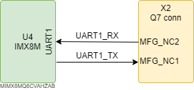
One UART_debug (UART1) interface is available on SOM-IMX8M_UQ7.
| Signal Name | Pin(s) | Direction | Voltage standard | Description | Connection |
|---|---|---|---|---|---|
| MFG_NC1 | 209 | out | 3V3 | Serial data line UART_TX for debugging. | U4.A7 |
| MFG_NC2 | 208 | in | 3V3 PU 10kΩ | Serial data line UART_RX for debugging. | U4.C7 |
One I2C (I2C1) interface (for communication between processor and peripherals) is available on SOM-IMX8M_UQ7.
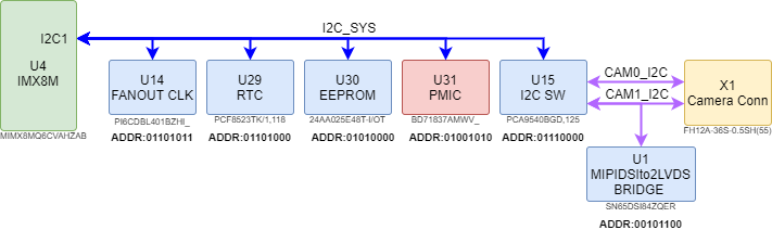
| Device | Address |
|---|---|
| PCIe clock buffer | 0x1101011 |
| RTC | 0x1101000 |
| EEPROM | 0x1010000 |
| PMIC | 0x1001010 |
| I2C-bus multiplexer | 0x1110000 |
| MIPIDSI→2LVDS bridge | 0x0101100 |
| Signal Name | Pin(s) | Direction | Voltage standard | Description | Comments |
|---|---|---|---|---|---|
| I2C1_CLK | E7 | in/out | 3V3 PU 4k7Ω | I2C Bus clock line. | |
| I2C1_SDA | E8 | in/out | 3V3 PU 4k7Ω | I2C Bus data line. |
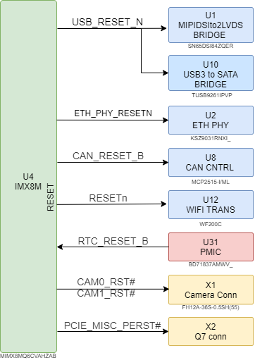
| Signal Name | Pin(s) | Voltage standard | Description | Connection |
|---|---|---|---|---|
| GPIO1_IO15 | J6 | 1V8 | ETH_PHY_RESETN | U2.42 |
| GPIO1_IO05 | P7 | 1V8 | CAM0_RST# | X1.11 |
| GPIO1_IO07 | N6 | 1V8 | CAM1_RST# | X1.31 |
| GPIO1_IO13 | K6 | 1V8 → 3V3 (U32) | USB_RESET_N | U1.42, U10.4 |
| RTC_RESET_B | W19 | 3V3 PU 10kΩ | RTC_RESET_B | U31.47 |
| SAI2_RXC | H3 | 3V3 PU 4k7Ω | CAN_RESET_B | U8.17 |
| SD1_RESET_N | R24 | 1V8 PU 10kΩ | RESETn | U12.15 |
| SAI5_MCLK | K4 | 3V3 | PCIE_MISC_PERST# | X2.158 |
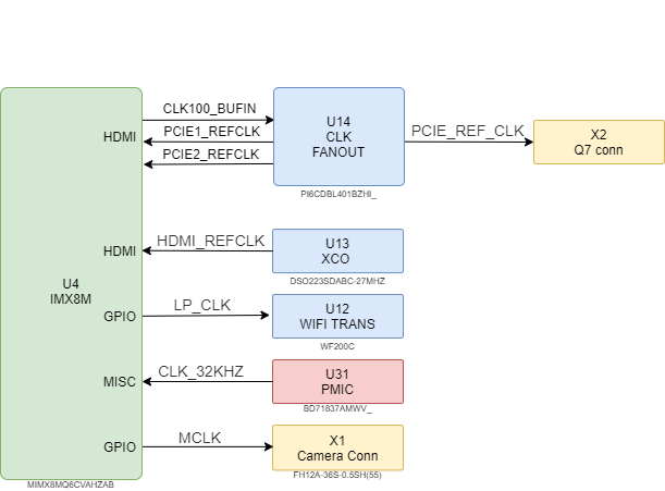
| Signal Name | Pin(s) | Voltage standard | Description | Connection |
|---|---|---|---|---|
| GPIO1_IO00 | T6 | LP_CLK | U12.23 | |
| GPIO1_IO14 | K7 | MCLK | X1.21 | |
| RTC | V22 | CLK_32kHz | U31.36 | |
| HDMI_REFCLK_P | R2 | HDMI_REFCLK_P | U13.4 (through 0 ohm) | |
| HDMI_REFCLK_N | R1 | HDMI_REFCLK_N | U13.5 (through 0 ohm) | |
| CLK2_O_P | T22 | CLK100_BUFIN_P | U14.5 | |
| CLK2_O_N | U22 | CLK100_BUFIN_N | U14.6 | |
| PCIE1_REF_PAD_CLK_P | K25 | PCIE1_REF_CLK_P | U14.18 | |
| PCIE1_REF_PAD_CLK_N | K24 | PCIE1_REF_CLK_N | U14.19 | |
| PCIE2_REF_PAD_CLK_P | F25 | PCIE2_REF_CLK_P | U14.13 | |
| PCIE2_REF_PAD_CLK_N | F24 | PCIE2_REF_CLK_N | U14.14 |
| Signal Name | Pin(s) | Voltage standard | Description | Connection |
|---|---|---|---|---|
| PCIE_REF_CLK_P | 155 | PCIE_REF_CLK_P | U14.22 (through 0 ohm) | |
| PCIE_REF_CLK_N | 157 | PCIE_REF_CLK_N | U14.23 (through 0 ohm) |
| Pins | Name (Bottom side row) | Signal group | Type | Comments | Pins | Name (Top side row) | Signal group | Type | Comments |
|---|---|---|---|---|---|---|---|---|---|
| 1 | GND | power | 2 | GND | power | ||||
| 3 | GBE_MDI3- | GBE | in/out | 4 | GBE_MDI2- | GBE | in/out | ||
| 5 | GBE_MDI3+ | GBE | in/out | 6 | GBE_MDI2+ | GBE | in/out | ||
| 7 | GBE_LINK100# | GBE | out | 8 | GBE_LINK1000# | GBE | out | ||
| 9 | GBE_MDI1- | GBE | in/out | 10 | GBE_MDI0- | GBE | in/out | ||
| 11 | GBE_MDI1+ | GBE | in/out | 12 | GBE_MDI0+ | GBE | in/out | ||
| 13 | GBE_LINK# | GBE | out | 14 | GBE_ACT# | GBE | out | ||
| 15 | GBE_CTREF | GBE | out | 16 | SUS_S5# | PWR_MGMT | out | ||
| 17 | WAKE# | PWR_MGMT | in | 18 | SUS_S3# | PWR_MGMT | out | ||
| 19 | GPO0(SUS_STAT#) | PWR_MGMT | out | 20 | PWRBTN# | PWR_MGMT | in | ||
| 21 | SLP_BTN#/GPII1 | PWR_MGMT | in | 22 | LID_BTN#/GPII0 | PWR_MGMT | in | ||
| 23 | GND | power | 24 | GND | power | ||||
| 25 | GND | power | 26 | PWGIN | PWR_MGMT | in | |||
| 27 | BATLOW#/GPII2 | PWR_MGMT | in | 28 | RSTBTN# | PWR_MGMT | in | ||
| 29 | SATA0_TX+ | SATA | out | 30 | SATA1_TX+ | SATA | out | ||
| 31 | SATA0_TX- | SATA | out | 32 | SATA1_TX- | SATA | out | ||
| 33 | SATA_ACT# | SATA | out | 34 | GND | power | |||
| 35 | SATA0_RX+ | SATA | in | 36 | SATA1_RX+ | SATA | in | ||
| 37 | SATA0_RX- | SATA | in | 38 | SATA1_RX- | SATA | in | ||
| 39 | GND | power | 40 | GND | power | ||||
| 41 | BIOS_DIS#/BOOT_ALT# | BOOT | in | 42 | SDIO_CLK# | SDIO | out | ||
| 43 | SDIO_CD# | SDIO | in/out | 44 | reserved (SDIO_LED) | ||||
| 45 | SDIO_CMD | SDIO | in/out | 46 | SDIO_WP | SDIO | in/out | ||
| 47 | SDIO_PWR# | SDIO | out | 48 | SDIO_DAT1 | SDIO | in/out | ||
| 49 | SDIO_DAT0 | SDIO | in/out | 50 | SDIO_DAT3 | SDIO | in/out | ||
| 51 | SDIO_DAT2 | SDIO | in/out | 52 | reserved (SDIO_DAT5) | ||||
| 53 | reserved (SDIO_DAT4) | 54 | reserved (SDIO_DAT7) | ||||||
| 55 | reserved (SDIO_DAT6) | 56 | USB_OTG_PEN (RSVD) | USB | out | ||||
| 57 | GND | power | 58 | GND | power | ||||
| 59 | HDA_SYNC/I2S_WS | AUDIO | out | 60 | SMB_CLK/GP1_I2C_CLK | MISC | in/out | ||
| 61 | HDA_RST#/I2S_RST# | AUDIO | out | 62 | SMB_DAT/GP1_I2C_DAT | MISC | in/out | ||
| 63 | HDA_BITCLK/I2S_CLK | AUDIO | out | 64 | SMB_ALERT# | MISC | in/out | ||
| 65 | HDA_SDI/I2S_SDI | AUDIO | in | 66 | GP0_I2C_CLK (I2C_CLK) | MISC | in/out | ||
| 67 | HDA_SDO/I2S_SDO | AUDIO | out | 68 | GP0_I2C_DAT (I2C_DAT) | MISC | in/out | ||
| 69 | THRM# | MISC | in | 70 | WDTRIG# | MISC | in | ||
| 71 | THRMTRIP# | MISC | out | 72 | WDOUT | MISC | out | ||
| 73 | GND | power | 74 | GND | power | ||||
| 75 | USB_P7-/USB_SSTX0- | USB | in/out | 76 | USB_P6-/USB_SSRX0- | USB | in/out | ||
| 77 | USB_P7+/USB_SSTX0+ | USB | in/out | 78 | USB_P6+/USB_SSRX0+ | USB | in/out | ||
| 79 | USB_6_7_OC# | USB | in | 80 | USB_4_5_OC# | USB | in | ||
| 81 | USB_P5-/USB_SSTX2- | USB | in/out | 82 | USB_P4-/USB_SSRX2- | USB | in/out | ||
| 83 | USB_P5+/USB_SSTX2+ | USB | in/out | 84 | USB_P4+/USB_SSRX2+ | USB | in/out | ||
| 85 | USB_2_3_OC# | USB | in | 86 | USB_0_1_OC# | USB | in | ||
| 87 | USB_P3- | USB | in/out | 88 | USB_P2- | USB | in/out | ||
| 89 | USB_P3+ | USB | in/out | 90 | USB_P2+ | USB | in/out | ||
| 91 | USB_VBUS (USB_CC) | USB | in | 92 | USB_ID | USB | in | ||
| 93 | USB_P1- | USB | in/out | 94 | USB_P0- | USB | in/out | ||
| 95 | USB_P1+ | USB | in/out | 96 | USB_P0+ | USB | in/out | ||
| 97 | GND | power | 98 | GND | power | ||||
| 99 | eDP0_TX0+/LVDS_A0+ | LVDS/eDP | out | 100 | eDP1_TX0+/LVDS_B0+ | LVDS/eDP | out | ||
| 101 | eDP0_TX0-/LVDS_A0- | LVDS/eDP | out | 102 | eDP1_TX0-/LVDS_B0- | LVDS/eDP | out | ||
| 103 | eDP0_TX1+/LVDS_A1+ | LVDS/eDP | out | 104 | eDP1_TX1+/LVDS_B1+ | LVDS/eDP | out | ||
| 105 | eDP0_TX1-/LVDS_A1- | LVDS/eDP | out | 106 | eDP1_TX1-/LVDS_B1- | LVDS/eDP | out | ||
| 107 | eDP0_TX2+/LVDS_A2+ | LVDS/eDP | out | 108 | eDP1_TX2+/LVDS_B2+ | LVDS/eDP | out | ||
| 109 | eDP0_TX2-/LVDS_A2- | LVDS/eDP | out | 110 | eDP1_TX2-/LVDS_B2- | LVDS/eDP | out | ||
| 111 | LVDS_PPEN | LVDS/eDP | out | 112 | LVDS_BLEN | LVDS/eDP | out | ||
| 113 | eDP0_TX3+/LVDS_A3+ | LVDS/eDP | out | 114 | eDP1_TX3+/LVDS_B3+ | LVDS/eDP | out | ||
| 115 | eDP0_TX3-/LVDS_A3- | LVDS/eDP | out | 116 | eDP1_TX3-/LVDS_B3- | LVDS/eDP | out | ||
| 117 | GND | power | 118 | GND | power | ||||
| 119 | eDP0_AUX+/LVDS_A_CLK+ | LVDS | out | 120 | eDP1_AUX+/LVDS_B_CLK+ | LVDS | in/out | ||
| 121 | eDP0_AUX-/LVDS_A_CLK- | LVDS | out | 122 | eDP1_AUX-/LVDS_B_CLK- | LVDS | in/out | ||
| 123 | LVDS_BLT_CTRL/GP_PWM_OUT0 | LVDS/eDP | out | 124 | GP_1-Wire_Bus/HDMI_CEC (RSVD) | HDMI/DP | in/out | ||
| 125 | LVDS_DID_DAT/GP_I2C_DAT | LVDS | in/out | 126 | eDP0_HPD#/LVDS_BLC_DAT | LVDS | in/out | ||
| 127 | LVDS_DID_CLK/GP_I2C_CLK | LVDS | in/out | 128 | eDP1_HPD#/LVDS_BLC_CLK | LVDS | in/out | ||
| 129 | CAN0_TX | CAN | out | 130 | CAN0_RX | CAN | in | ||
| 131 | DP_LANE3+/TMDS_CLK+ (SDVO_BCLK+) | HDMI/DP | out | 132 | USB_SSTX1- (SDVO_INT+) | USB | out | ||
| 133 | DP_LANE3-/TMDS_CLK- (SDVO_BCLK-) | HDMI/DP | out | 134 | USB_SSTX1+ (SDVO_INT-) | out | |||
| 135 | GND | power | 136 | GND | power | ||||
| 137 | DP_LANE1+/TMDS_LANE1+ (SDVO_GREEN+) | HDMI/DP | out | 138 | DP_AUX+ (SDVO_FLDSTALL+) | DP | in/out | ||
| 139 | DP_LANE1-/TMDS_LANE1- (SDVO_GREEN-) | HDMI/DP | out | 140 | DP_AUX- (SDVO_FLDSTALL-) | DP | in/out | ||
| 141 | GND | power | 142 | GND | power | ||||
| 143 | DP_LANE2+/TMDS_LANE0+ (SDVO_BLUE+) | HDMI/DP | out | 144 | USB_SSRX1- (SDVO_TVCLKIN+) | USB | in | ||
| 145 | DP_LANE2-/TMDS_LANE0- (SDVO_BLUE-) | HDMI/DP | out | 146 | USB_SSRX1+ (SDVO_TVCLKIN-) | USB | in | ||
| 147 | GND | power | 148 | GND | power | ||||
| 149 | DP_LANE0+/TMDS_LANE2+ (SDVO_RED+) | HDMI/DP | out | 150 | HDMI_CTRL_DAT (SDVO_CTRL_DAT) | HDMI/DP | in/out | ||
| 151 | DP_LANE0-/TMDS_LANE2- (SDVO_RED-) | HDMI/DP | out | 152 | HDMI_CTRL_CLK (SDVO_CTRL_CLK) | HDMI/DP | in/out | ||
| 153 | HDMI_HPD# | HDMI/DP | Вход | 154 | DP_HPD# | DP | in | ||
| 155 | PCIE_CLK_REF+ | PCI-E | out | 156 | PCIE_WAKE# | PCI-E | in | ||
| 157 | PCIE_CLK_REF- | PCI-E | out | 158 | PCIE_RST# | PCI-E | out | ||
| 159 | GND | power | 160 | GND | power | ||||
| 161 | PCIE3_TX+ | PCI-E | out | 162 | PCIE3_RX+ | PCI-E | in | ||
| 163 | PCIE3_TX- | PCI-E | out | 164 | PCIE3_RX- | PCI-E | in | ||
| 165 | GND | power | 166 | GND | power | ||||
| 167 | PCIE2_TX+ | PCI-E | out | 168 | PCIE2_RX+ | PCI-E | in | ||
| 169 | PCIE2_TX- | PCI-E | out | 170 | PCIE2_RX- | PCI-E | in | ||
| 171 | UART0_TX (EXCD0_PERST#) | UART | out | 172 | UART0_RTS# (EXCD1_PERST#) | UART | out | ||
| 173 | PCIE1_TX+ | PCI-E | out | 174 | PCIE1_RX+ | PCI-E | in | ||
| 175 | PCIE1_TX- | PCI-E | out | 176 | PCIE1_RX- | PCI-E | in | ||
| 177 | UART0_RX (EXCD0_CPPE#) | UART | in | 178 | UART0_CTS# (EXCD1_CPPE#) | UART | in | ||
| 179 | PCIE0_TX+ | PCI-E | out | 180 | PCIE0_RX+ | PCI-E | in | ||
| 181 | PCIE0_TX- | PCI-E | out | 182 | PCIE0_RX- | PCI-E | in | ||
| 183 | GND | power | 184 | GND | power | ||||
| 185 | LPC_AD0/GPIO0 | LPC | in/out | 186 | LPC_AD1/GPIO1 | LPC | in/out | ||
| 187 | LPC_AD2/GPIO2 | LPC | in/out | 188 | LPC_AD3/GPIO3 | LPC | in/out | ||
| 189 | LPC_CLK/GPIO4 | LPC | in/out | 190 | LPC_FRAME#/GPIO5 | LPC | in/out | ||
| 191 | SERIRQ/GPIO6 | LPC | in/out | 192 | LPC_LDRQ#/GPIO7 | LPC | in/out | ||
| 193 | VCC_RTC | in | 194 | SPKR/GP_PWM_OUT2 | out | ||||
| 195 | FAN_T_IN/GP_TIMER_IN | MISC | in | 196 | FAN_OUT/GP_PWM_OUT1 | MISC | out | ||
| 197 | GND | power | 198 | GND | power | ||||
| 199 | SPI_MOSI | SPI | out | 200 | SPI_CS0# | SPI | out | ||
| 201 | SPI_MISO | SPI | in | 202 | SPI_CS1# | SPI | out | ||
| 203 | SPI_SCK | SPI | out | 204 | MFG_NC4 | MFG | in | ||
| 205 | VCC_5V_SB | in | 206 | VCC_5V_SB | in | ||||
| 207 | MFG_NC0 | MFG | in | 208 | MFG_NC2 | MFG | in | ||
| 209 | MFG_NC1 | MFG | out | 210 | MFG_NC3 | MFG | in | ||
| 211 | NC (VCC) | 212 | NC (VCC) | ||||||
| 213 | NC (VCC) | 214 | NC (VCC) | ||||||
| 215 | NC (VCC) | 216 | NC (VCC) | ||||||
| 217 | NC (VCC) | 218 | NC (VCC) | ||||||
| 219 | VCC | in | 220 | VCC | in | ||||
| 221 | VCC | in | 222 | VCC | in | ||||
| 223 | VCC | in | 224 | VCC | in | ||||
| 225 | VCC | in | 226 | VCC | in | ||||
| 227 | VCC | in | 228 | VCC | in | ||||
| 229 | VCC | in | 230 | VCC | in |
