Инструменты пользователя
Боковая панель
Это старая версия документа!
Содержание
DCDC
Snubber
Snubber - цепочка, компенсирующая паразитные L и C в DCDC.
- Резистор может прилично греться
- Надо подбирать экспериментально
Про snubber:
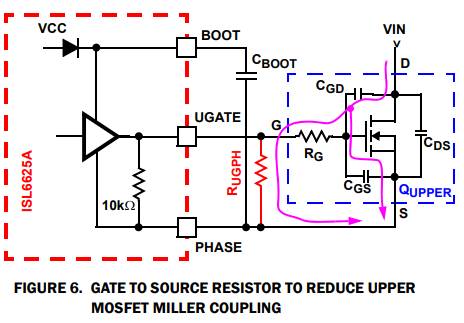
MOSFET Self-Turn-On Phenomenon
Эффект произвольного включения верхнего транзистора.
Про эффект:
Из даташита ISL6625A:
Should the driver have insufficient bias voltage applied, its
outputs are floating. If the input bus is energized at a high dV/dt
rate while the driver outputs are floating, due to self-coupling via
the internal CGD of the MOSFET, the gate of the upper MOSFET
could momentarily rise up to a level greater than the threshold
voltage of the device, potentially turning on the upper switch.
Therefore, if such a situation could conceivably be encountered,
it is a common practice to place a resistor (RUGPH) across the
gate and source of the upper MOSFET to suppress the Miller
coupling effect. The value of the resistor depends mainly on the
input voltage’s rate of rise, the CGD/CGS ratio, as well as the
gate-source threshold of the upper MOSFET. A higher dV/dt, a
lower CDS/CGS ratio, and a lower gate-source threshold upper
FET will require a smaller resistor to diminish the effect of the
internal capacitive coupling. For most applications, the
integrated 20kΩ resistor is sufficient, not affecting normal
performance and efficiency.
The coupling effect can be roughly estimated with Equation 5, which assumes a fixed linear input ramp and neglects the clamping effect of the body diode of the upper drive and the bootstrap capacitor. Other parasitic components such as lead inductances and PCB capacitances are also not taken into account. Figure 6 provides a visual reference for this phenomenon and its potential solution.


