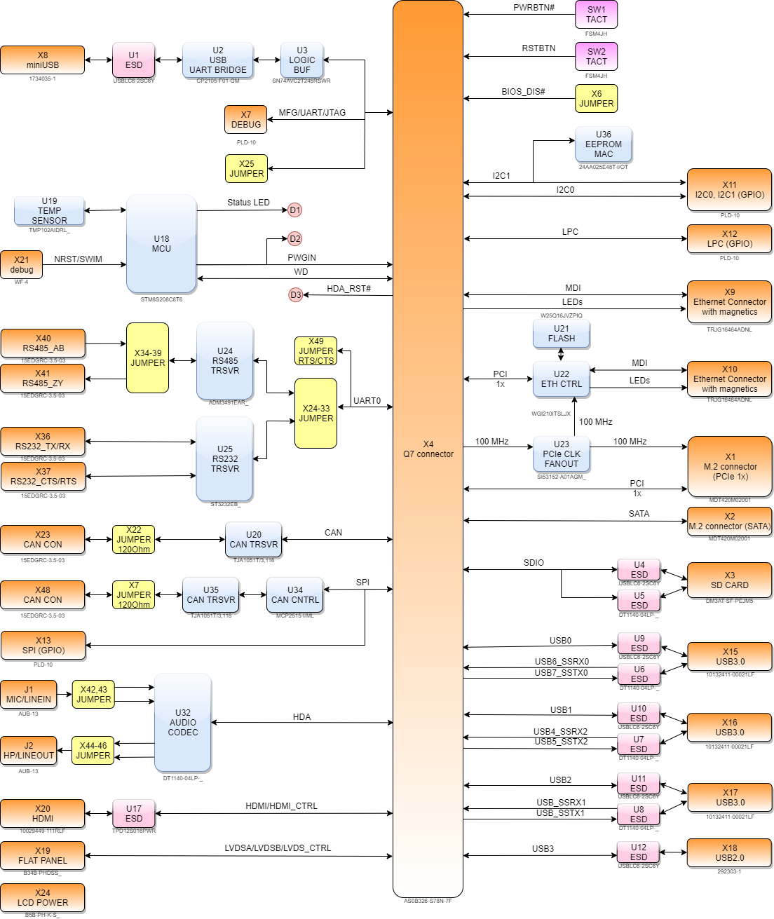

Main technical specifications
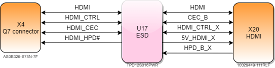
| Video Interfaces | HDMI interface |
|---|---|
| Video Resolutions | HDMI resolution up to 4k@60Hz |
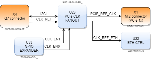
| Mass Storage | 1 x S-ATA channel (M.2 connector) |
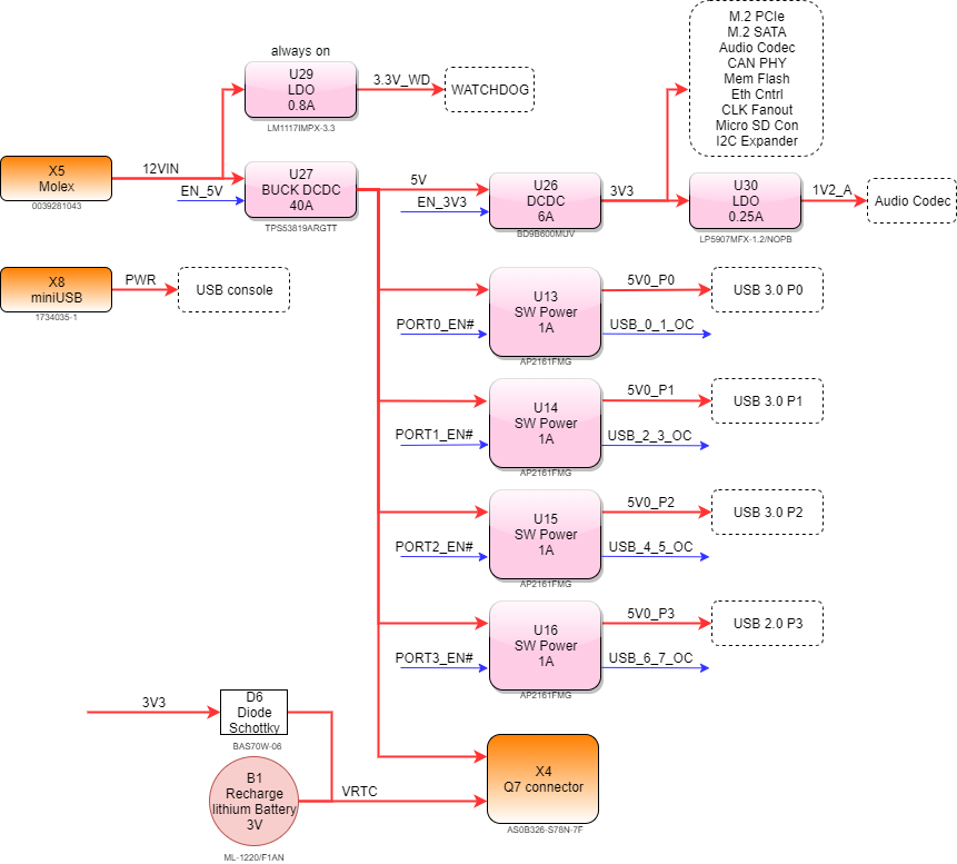
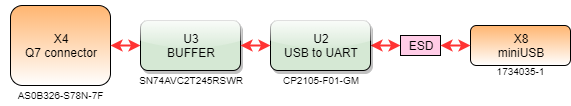
| USB | - 3 x USB 3.0 - 1 x USB 2.0 - 1 x mini USB (USB to UART console) |
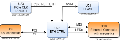
| Networking | - Gigabit Ethernet interface (from Q7 SOM Ethernet PHY) - Gigabit Ethernet interface (from onboard Intel WGI210ITSLJX PCIe Gigabit Ethernet PHY) |
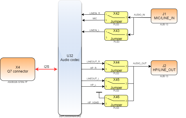
| Audio | - Audio 3.5 mm jack (Line in\Mic in) - Audio 3.5 mm jack (Line out\Headphones) |
| PCI Express | 2 x PCI-e 1x: - one routed to M.2 Connector - one routed to Intel WGI210ITSLJX PCIe Gigabit Ethernet PHY |
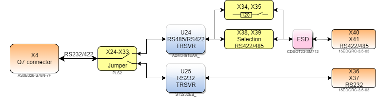
| Serial Ports | 1 x Serial port (RS-232/RS-485/RS-422) 1 x Debug console (UART to USB) |
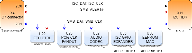
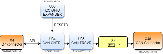
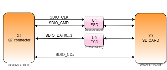
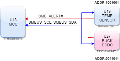
| Other Interfaces | - 1 x CAN interface - 2 x I2C interface - 1 x SPI interface - 1 x LPC interface (8 GPIO) |
| Power supply voltage | +12 VDC |
| Power consumption | TBD |
| Operating temperature | -40°C…+85°C |
| Dimensions: | 147 x 101.60 mm |